ISSN (Online) : 2278-1021
ISSN (Print) : 2319-5940
International Journal of Advanced Research in Computer and Communication Engineering
Vol. 3, Issue 10, October 2014
Implementation of Ripple Carry and Carry Skip
Adders with Speed and Area Efficient
PUSHPALATHA CHOPPA1, B.N. SRINIVASA RAO2
PG Scholar (VLSI Design), Department of ECE, Avanthi Institute of Engineering & Tech., Visakhapatnam,AP, India 1
Associate Professor, Department of ECE, Avanthi Institute of Engineering & Technology, Visakhapatnam, AP, India 2
Abstract: The binary adder is the critical element in most digital circuit designs including digital signal processors
(DSP) and microprocessor datapath units. As such, extensive research continues to be focused on improving the
powerdelay performance of the adder. In VLSI implementations, parallel-prefix adders are known to have the best
performance. Binary adders are one of the most essential logic elements within a digital system. In addition, binary
adders are also helpful in units other than Arithmetic Logic Units (ALU), such as multipliers, dividers and memory
addressing. Therefore, binary addition is essential that any improvement in binary addition can result in a performance
boost for any computing system and, hence, help improve the performance of the entire system. Parallel-prefix adders
(also known as carry-tree adders) are known to have the best performance in VLSI designs. This paper investigates
three types of carry-tree adders (the Kogge-Stone, sparse Kogge-Stone, and spanning tree adder) and compares them to
the simple Ripple Carry Adder (RCA) and Carry Skip Adder (CSA). In this project Xilinx-ISE tool is used for
simulation,logical verification, and further synthesizing.
Keywords: Include at least 4 keywords or phrases
I. INTRODUCTION
Binary adders are one of the most essential logic elements
within a digital system. In addition, binary adders are also
helpful in units other than Arithmetic Logic Units (ALU),
such as multipliers, dividers and memory addressing.
Therefore, binary addition is essential that any
improvement in binary addition can result in a
performance boost for any computing system and, hence,
help improve the performance of the entire system.
The major problem for binary addition is the carry chain.
As the width of the input operand increases, the length of
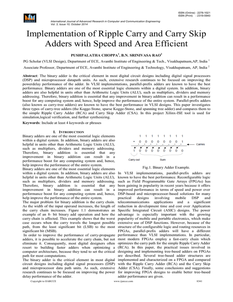
the carry chain increases. Figure 1.1 demonstrates an
example of an 8- bit binary add operation and how the
carry chain is affected. This example shows that the worst
case occurs when the carry travels the longest possible
path, from the least significant bit (LSB) to the most
significant bit (MSB).
In order to improve the performance of carry-propagate
adders, it is possible to accelerate the carry chain, but not
eliminate it. Consequently, most digital designers often
resort to building faster adders when optimizing a
computer architecture, because they tend to set the critical
path for most computations.
The binary adder is the critical element in most digital
circuit designs including digital signal processors (DSP)
and microprocessor data path units. As such, extensive
research continues to be focused on improving the power
delay performance of the adder.
Copyright to IJARCCE
Fig.1. Binary Adder Example.
In VLSI implementations, parallel-prefix adders are
known to have the best performance. Reconfigurable logic
such as Field Programmable Gate Arrays (FPGAs) has
been gaining in popularity in recent years because it offers
improved performance in terms of speed and power over
DSP-based and microprocessor-based solutions for many
practical designs involving mobile DSP and
telecommunications applications and a significant
reduction in development time and cost over Application
Specific Integrated Circuit (ASIC) designs. The power
advantage is especially important with the growing
popularity of mobile and portable electronics, which make
extensive use of DSP functions. However, because of the
structure of the configurable logic and routing resources in
FPGAs, parallel-prefix adders will have a different
performance than VLSI implementations. In particular,
most modern FPGAs employ a fast-carry chain which
optimizes the carry path for the simple Ripple Carry Adder
(RCA). In this paper, the practical issues involved in
designing and implementing tree-based adders on FPGAs
are described. Several tree-based adder structures are
implemented and characterized on a FPGA and compared
with the Ripple Carry Adder (RCA) and the Carry Skip
Adder (CSA). Finally, some conclusions and suggestions
for improving FPGA designs to enable better tree-based
adder performance are given.
www.ijarcce.com
8341
ISSN (Online) : 2278-1021
ISSN (Print) : 2319-5940
International Journal of Advanced Research in Computer and Communication Engineering
Vol. 3, Issue 10, October 2014
The implementations that have been developed in this
dissertation help to improve the design of parallel- prefix
adders and their associated computing architectures. This
has the potential of impacting many application specific
and
general
purpose
computer
architectures.
Consequently, this work can impact the designs of many
computing systems, as well as impacting many areas of
engineers and science. In this paper, the practical issues
involved in designing and implementing tree-based adders
on FPGAs are described. Several tree-based adder
structures are implemented and characterized on a FPGA
and compared with the Ripple Carry Adder (RCA) and the
Carry Skip Adder (CSA). Finally, some conclusions and
suggestions for improving FPGA designs to enable better
tree-based adder performance are given.
different functionality. The input lines to the logic block
go into the LUT and enable it. The output of the LUT
gives the result of the logic function that it implements and
the output of logic block is registered or unregistered
output from the LUT. SRAM is used to implement a
LUT.A k-input logic function is implemented using 2^k *
1 size SRAM. Number of different possible functions for k
input LUT is 2^2^k. Advantage of such an architecture is
that it supports implementation of so many logic functions,
however the disadvantage is unusually large number of
memory cells required to implement such a logic block in
case number of inputs is large.
A simplified version of design flow is given in the flowing
diagram as shown in fig.3.
II. FPGA IMPLEMENTATION AND DESIGN FLOW
FPGA contains a two dimensional arrays of logic blocks
and interconnections between logic blocks. Both the logic
blocks and interconnects are programmable. Logic blocks
are programmed to implement a desired function and the
interconnections are programmed using the switch boxes
to connect the logic blocks. To be more clear, if we want
to implement a complex design (CPU for instance), then
the design is divided into small sub functions and each sub
function is implemented using one logic block. Now, to
get our desired design (CPU), all the sub functions
implemented in logic blocks must be connected and this is
done by programming the internal structure of an FPGA
which is depicted in the following figure 1.2
Fig.3. FPGA Design Flow
There are different techniques for design entry. Schematic
based, Hardware Description Language and combination
of both etc. . Selection of a method depends on the design
and designer. If the designer wants to deal more with
Hardware, then Schematic entry is the better choice. When
the design is complex or the designer thinks the design in
an algorithmic way then HDL is the better choice.
Language based entry is faster but lag in performance and
density.HDLs represent a level of abstraction that can
isolate the designers from the details of the hardware
implementation. Schematic based entry gives designers
much more visibility into the hardware. It is the better
choice for those who are hardware oriented. Another
method but rarely used is state-machines. It is the better
Fig. 2: FPGA interconnections
choice for the designers who think the design as a series of
FPGAs, alternative to the custom ICs, can be used to states. But the tools for state machine entry are limited. In
implement an entire System On one Chip (SOC). The this documentation we are going to deal with the HDL
main advantage of FPGA is ability to reprogram. User can based design entry.
reprogram an FPGA to implement a design and this is
done after the FPGA is manufactured. This brings the
name “Field Programmable.” Custom ICs are expensive
and takes long time to design so they are useful when
produced in bulk amounts. But FPGAs are easy to
implement within a short time with the help of Computer
Aided Designing (CAD) tools (because there is no
physical layout process, no mask making, and no IC
manufacturing). Some disadvantages of FPGAs are, they
are slow compared to custom ICs as they can’t handle vary
complex designs and also they draw more power. Xilinx
logic block consists of one Look Up Table (LUT) and one
Fig.4. FPGA Synthesis
Flip-Flop. An LUT is used to implement number of
Copyright to IJARCCE
www.ijarcce.com
8342
ISSN (Online) : 2278-1021
ISSN (Print) : 2319-5940
International Journal of Advanced Research in Computer and Communication Engineering
Vol. 3, Issue 10, October 2014
The process that translates VHDL/ Verilog code into a
device netlist format i.e. a complete circuit with logical
elements (gates flip flop, etc…) for the design. If the
design contains more than one sub designs, ex. to
implement a processor, we need a CPU as one design
element and RAM as another and so on, then the synthesis
process generates netlist for each design element
Synthesis process will check code syntax and analyze the
hierarchy of the design which ensures that the design is
optimized for the design architecture, the designer has
selected. The resulting netlist(s) is saved to an NGC
(Native Generic Circuit) file (for Xilinx® Synthesis
Technology (XST)).
III. EXISTING METHODS
Ripple-Carry Adders (RCA)
The simplest way of doing binary addition is to connect
the carry-out from the previous bit to the next bit's carryin. Each bit takes carry-in as one of the inputs and outputs
sum and carry-out bit and hence the name ripple-carry
adder. This type of adders is built by cascading 1-bit full
adders. A 4-bit ripple-carry adder is shown in Figure 2.3.
Each trapezoidal symbol represents a single-bit full adder.
At the top of the figure, the carry is rippled through the
adder from cin to cout.
It can be observed in Figure 3.1 that the critical path,
highlighted with a solid line, is from the least significant
bit (LSB) of the input (a0 or b0) to the most significant bit
(MSB) of sum (sn-1). The ripple carry adder is
constructed by cascading full adders (FA) blocks in
series. One full adder is responsible for the addition of
two binary digits at any stage of the ripple carry. The
carryout of one stage is fed directly to the carry-in of the next
stage.
Fig.5.Ripple-Carry Adder[13].
Assuming each simple gate, including AND, OR and XOR
gate has a delay of 2/\ and NOT gate has a delay of 1/\. All
the gates have an area of 1 unit. Using this analysis and
assuming that each add block is built with a 9-gate full
adder, the critical path is calculated as follows.
ai , bi si = 10/\
ai , bi ci+1 = 9/\
ci si = 5/\
ci ci+1 = 4/\
The critical path, or the worst delay is
trca = {9 + (n- 2) x 4 + 5}/\ = {f4n + 6}/\
As each bit takes 9 gates, the area is simply 9n for a n-bit
RCA.
Copyright to IJARCCE
Carry-Select Adders (CSEA)
Simple adders, like ripple-carry adders, are slow since the
carry has to to travel through every full adder block. There
is a way to improve the speed by duplicating the hardware
due to the fact that the carry can only be either 0 or 1. The
method is based on the conditional sum adder and
extended to a carry-select adder. With two RCA, each
computing the case of the one polarity of the carry-in, the
sum can be obtained with a 2x1 multiplexer with the
carry-in as the select signal. An example of 16-bit carryselect adder is shown in Figure 3.2. In the figure, the adder
is grouped into four 4-bit blocks. The 1-bit multiplexors
for sum selection can be implemented as Figure 3.2 shows.
Assuming the two carry terms are utilized such that the
carry input is given as a constant 1 or 0:
Fig.6. Carry-Select Adder[13]
In Fig.6, each two adjacent 4-bit blocks utilizes a carry
relationship
ci+4 = c0 i+4 + c1 i+4 . ci
Temporary sums can be defined as follows.
s0 i+1 = ti+1 . c0 i
s1 i+1 = ti+1 . c1 i
The final sum is selected by carry-in between the
temporary sums already calculated.
si+1 = cj . s0 i+1 + cj . s1 i+1
Assuming the block size is fixed at r-bit, the n-bit adder is
composed of k groups of r-bit blocks, i.e. n = r x k.
The critical path with the first RCA has a delay of (4r +
5)/\ from the input to the carry-out, and there are k - 2
blocks that follow, each with a delay of 4/\ for carry to go
through. The final delay comes from the multiplexor,
which has a delay of 5/\, as indicated in Figure 2.5. The
total delay for this CSEA is calculated as
tcsea = 4r + 5 + 4(k - 2) + 5/\ = {4r + 4k + 2}/\
The area can be estimated with (2n - r) FAs, (n - r)
multiplexors and (k - 1) AND/OR logic. As mentioned
above, each FA has an area of 9 and a multiplexor takes 5
units of area. The total area can be estimated
9(2n - r) + 2(k - 1) + 4(n - r) = 22n - 13r + 2k - 2
The delay of the critical path in CSEA is reduced at the
cost of increased area. For example, in Figure 3.2, k = 4, r
= 4 and n = 16. The delay for the CSEA is 34/\ compared
to 70/\ for 16-bit RCA. The area for the CSEA is 310 units
while the RCA has an area of 144 units.
The delay of the CSEA is about the half of the RCA. But
the CSEA has an area more than twice that of the RCA.
Each adder can also be modified to have a variable block
sizes, which gives better delay and slightly less area.
Carry-Skip Adders (CSKA)
There is an alternative way of reducing the delay in the
carry-chain of a RCA by checking if a carry will propagate
through to the next block. This is called carry-skip adder
ci+1 = Pi:j _ Gi:j + Pi:j . cj
www.ijarcce.com
8343
ISSN (Online) : 2278-1021
ISSN (Print) : 2319-5940
International Journal of Advanced Research in Computer and Communication Engineering
Vol. 3, Issue 10, October 2014
fig.7. Carry-Skip Adder[13]
The carry-out of each block is determined by selecting the
carry-in and Gi:j using Pi:j. When Pi:j = 1, the carry-in cj
is allowed to get through the block immediately.
Otherwise, the carry-out is determined by Gi:j. The CSKA
has less delay in the carry-chain with only a little
additional extra logic.
Further improvement can be achieved generally by
making the central block sizes larger and the two-end
block sizes smaller.
Assuming the n-bit adder is divided evenly to k r-bit
blocks, part of the critical path is from the LSB input
through the MSB output of the final RCA.
The first delay is from the LSB input to carry-out, which is
4r + 5. Then, there are k - 2 skip logic blocks with a delay
of 3/\. Each skip logic block includes one 4-input AND
gate for getting Pi+3:i and one AND/OR logic.
The final RCA has a delay from input to sum at MSB,
which is 4r+6. The total delay is calculated as follows.
tcska
= {4r + 5 + 3(k - 2) + 4r + 6}/\
= {8r + 3k + 5}/\
The CSKA has n-bit FA and k - 2 skip logic blocks. Each
skip logic block has an area of 3 units. Therefore, the total
area is estimated as 9n + 3(k - 2) = 9n + 3k – 6.
Fig.9. Kogeee stone 32 bit
Fig.10.Kogeee stone 64 bit
IV. RESULTS
The results pertaining to the proposed work are given in
this section. Output representation regarding koggee stone
algorithm for 16 bit, 32 bit and 64 bit are presented in
Fig.8 through Fig.10.
Results involving implementation of RCA 16 bit, RCA 32
bit and RCA 64 bit and Carry Skip for 16 bit, carry skip 32
bit and carry skip 64 are presented in the subsequent
figures.
Fig.8. Koggee stone 16 bit
Copyright to IJARCCE
Fig.11.Rca 16 bit adder
Fig.12.Rca 32 bit adder
www.ijarcce.com
8344
ISSN (Online) : 2278-1021
ISSN (Print) : 2319-5940
International Journal of Advanced Research in Computer and Communication Engineering
Vol. 3, Issue 10, October 2014
V. CONCLUSION
The results presented in the preceding section significantly
produced the efficiency of the proposed methodology. The
performance evaluation of the simulated models would be
good starting point of further research.
REFERENCES
[1]
[2]
Fig.12.Rca 64 bit adder
[3]
[4]
[5]
[6]
[7]
[8]
[9]
Fig.13.Carry skip 16 bit
P. Ndai, S. Lu, D. Somesekhar, and K. Roy, “Fine-Grained
Redundancy in Adders,” Int. Symp. on QualityElectronic Design,
pp. 317-321, March 2007.
T. Lynch and E. E. Swartzlander, “A Spanning Tree Carry
Lookahead Adder,” IEEE Trans. on Computers, vol. 41, no. 8, pp.
931-939, Aug. 1992.
D. Gizopoulos, M. Psarakis, A. Paschalis, and Y. Zorian, “Easily
Testable Cellular Carry Lookahead Adders,” Journal of Electronic
Testing: Theory and Applications 19, 285-298, 2003.
S. Xing and W. W. H. Yu, “FPGA Adders: Performance Evaluation
and Optimal Design,” IEEE Design & Test of Computers, vol. 15,
no. 1, pp. 24-29, Jan. 1998.
M. Bečvář and P. Štukjunger, “Fixed-Point Arithmetic in FPGA,”
Acta Polytechnica, vol. 45, no. 2, pp. 67-72, 2005.
N. H. E. Weste and D. Harris, CMOS VLSI Design, 4th edition,
Pearson–Addison-Wesley, 2011.
R. P. Brent and H. T. Kung, “A regular layout for parallel adders,”
IEEE Trans. Comput., vol. C-31, pp. 260-264, 1982.
D. Harris, “A Taxonomy of Parallel Prefix Networks,” in Proc. 37th
Asilomar Conf. Signals Systems and Computers, pp. 2213–7, 2003.
P. M. Kogge and H. S. Stone, “A Parallel Algorithm for the
Efficient Solution of a General Class of Recurrence Equations,”
IEEE Trans. on Computers, Vol. C-22, No 8, August 1973
Fig.14.Carry skip 32 bit:
Fig.14.Carry skip 64 bit
Copyright to IJARCCE
www.ijarcce.com
8345


