Filter circuits having transformers as filter elements
advertisement
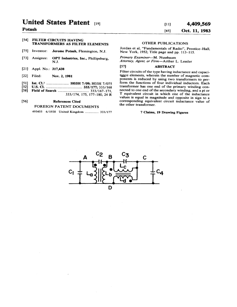
O Umted States Patent [191 [11] 4,409,569 Potash [45] Oct. 11, 1983 [54] FILTER CIRCUITS HAVING TRANSFORMERS AS FILTER ELEMENTS [75] Inventor: - Jerome Potash, Flemington, NJ. , - [73] Asslgnee' - - Industries’ Inc" phlnlpsburg’ OTHER PUBLICATIONS Jordan et al, "Fundamentals of Radio”, Prentice-Hall, New York, 1952; Title page and pp. 1l3—l l5. Primary Examiner—-M. Nussbaum Attorney. Agent, or Firm-Arthur L. Lessler [57] [2]] App!‘ NO': 3"’438 [22] Filed Nov 2 1981 ' ' ABSTRACT Filter circuits of the type having inductance and capaci tmce elements, wherein the number of magnetic com ’ ponents is reduced by using two transformers to per lnt. GL3 7/09, 7/075 [52] us. Cl. ............................. 335/177‘ 333/168 form Th8 fIlIlCliOIlS 0f four individual II'ldUCIOI'S. Each transfmme' has One end 01" the Primary winding C0“ [581 "wed ‘0 one end of the sewndary winding’ and a Pi °r Field of Search .............................. .. 333}167-l71 333/174 175 177480 24 ’ [56] ’ ' References Cited 6/1938 United Kingdom values is equal in magnitude and opposite in sign to a corresponding equivalent circuit inductance value of the other transformer. FOREIGN PATENT DOCUMENTS 495455 T equivalent circuit in which one of the inductance 333/177 7 Claims, 19 Drawing Figures US. Patent 0m. 11, 1983 Sheet 2 0M Ac2BC3 w.‘ LC IILG"LbLd. D FIG.5 c T4c . 4,409,569 US. Patent 0a. 11, 1983 Sheet 3 of4 a-35-5,3 Q635:lL FIm _QM WUYEN row .Tm QH45W_EN._OJ |,| h AmOEn: w.0_|. 0.0K 4,409,569 1 4,409,569 2 ?lter according to a ?rst embodiment of the present FILTER CIRCUITS HAVING TRANSFORMERS AS FILTER ELEMENTS BACKGROUND OF THE INVENTION invention; FIG. 5 shows a ?lter according to said ?rst embodi ment of the invention; FIG. 6 illustrates an intermediate step (in conjunction 5 with FIGS. 2, 3(0), 3(b), and 4(b) in converting the ?lter This invention relates to electric ?lter circuits and processes for manufacturing the same, and more partic ularly to ?lters which include a number of inductors. In the design of ?lters having desired frequency re sponse characteristics, it is frequently necessary or de sirable to include a number of individual inductors. of FIG. 1 to a ?lter according to a second embodiment of the present invention; FIG. 7 shows a ?lter according to said second em bodiment of the invention; FIG. 8 shows a second type of prior art ?lter; having more than four inductance elements; FIG. 9 shows an intermediate step in converting the Such inductors are relatively expensive magnetic com ponents and occupy a relatively large volume. Accordingly, an object of the present invention is to provide ?lter circuits having desired frequency re sponse characteristics similar to those of prior art ?lters ?lter of FIG. 8 to a ?lter according to a third embodi ment of the present invention; FIG. 10 shows a ?lter according to said third embodi ment of the invention; FIG. 11 shows a third type of prior art ?lter having four inductance elements; of the aforementioned type, at reduced cost and in a smaller space. SUMMARY 20 FIGS. 12, 13(0), 13(b), 14(0) and 14(b) show interme diate steps in converting the ?lter of FIG. 11 to a ?lter according to a fourth embodiment of the present inven As herein described, there is provided an improved ?lter circuit comprising at least two transformers and tion; and FIG. 15 shows a ?lter according to said fourth em‘ having a frequency characteristic corresponding to that of a given ?lter circuit including at least four individual 25 bodiment of the invention. inductors, comprising a pair of transformers each hav DETAILED DESCRIPTION ing a T or pi network equivalent circuit wherein two The present invention, as hereinafter described in inductance values correspond to those of two of said further detail, utilizes two transformers (or more than individual inductors, the third inductance value of one one group of two transformers) having parameters such of said equivalent circuits being positive and the third that they provide frequency response characteristics inductance value of the other of said equivalent circuits similar to those of four individual inductors, thus reduc being negative and equal to the third inductance value ing the number of individual magnetic components by of the ?rst-mentioned of said equivalent circuits, said transformers being interconnected so that said equiva two, resulting in a saving of cost and of space occupied lent circuit third inductance values are in series or in 35 by the ?lter. One of the two transformers has its windings coupled in series aiding relationship [as shown for example in parallel with each other, whereby the third inductance values do not affect the frequency characteristic of said ?lter circuit. Also herein described is a process for manufacturing an improved ?lter circuit comprising at least two trans formers and having a frequency characteristic corre sponding to that of a given ?lter circuit including at least four individual inductors, comprising the steps of: representing said given circuit schematically; adding to the representation of said ?lter circuit a pair of positive and negative interim inductors having equal absolute values of inductance, the inductors of said pair being coupled in series or in parallel with each other so that FIG. 4(b)], so that the mutual inductance m between the primary and secondary windings has a negative sign; the other transformer having its windings coupled in series opposing relationship [as shown for example in FIG. 4(0)], 80 that the mutual inductance therebetween 45 has a positive sign. In this arrangement, the equivalent circuit of one transformer has two positive inductance values and one negative inductance value (see FIG. 3(b), for example), while the equivalent circuit of the other transformer has three positive inductance values (see FIG. 3(a), for example). By properly setting the design parameters of each the frequency characteristic of said ?lter circuit is not 50 transformer, and the manner in which the transformers altered thereby, and so that each inductor of said pair are interconnected, the negative equivalent circuit in cooperates with two adjacent individual inductors to ductance value of one transformer may be "cancelled form a T or pi network, wherein in each such network out” by one of the inductance values of the equivalent the absolute value of the inductance of the correspond circuit of the other transformer, thus resulting in an ing interim inductor is less than the square root of the equivalent circuit comprising four inductors. The trans product of the inductances of the individual inductors formers can be so designed that their combined equiva therein; and fabricating said improved ?lter circuit by lent circuit, comprising four inductors, has the same inductance values as those of the four individual induc providing a transformer to perform the function of each tors of the prior art ?lter circuit. of said networks, each such transformer having an A ?rst embodiment of the invention based on these equivalent circuit corresponding to that of the respec principles is shown in FIG. 5, which circuit has a fre tive network. quency characteristic similar to that of the prior art IN THE DRAWING circuit shown in FIG. 1. In converting the circuit of FIG. 1 to that of FIG. 5, FIG. 1 shows a ?rst type of ?lter circuit according to the prior art, having four individual inductance ele 65 two parallel inductors are added to the schematic repre sentation of FIG. 1, said inductors having inductance ments or inductors; FIGS. 2, 3(a), 3(1)), 4(0) and 4(b) illustrate intermedi ate steps in converting the prior art ?lter of FIG. 1 to a values +L and —L respectively. The positioning of the added positive and negative inductance values is se 3 4,409,569 4 lected, as shown in FIG. 2, so that each of said added inductance values forms a delta or pi network with two Le : adjacent individual inductors of the original prior art (38) circuit. As seen in FIG. 2, the inductance value +L forms a ?rst pi network with individual inductors L1 and L2; while the inductance value —L forms a second pi network with individual inductors L3 and L4. These pi networks are shown in FIGS. 3(a) and 3(b) respec (3c) tively. The pi network shown in FIG. 3(a) is then replaced by the transformer shown in FIG. 4(a), said transformer and the resulting circuit is as shown in FIG. 7. A somewhat more complex prior art circuit is shown in FIG. 8, which conduit includes seven individual having primary and secondary windings La and Lb connected in series opposing relationship to provide a positive sign for the mutual inductance mab therebe inductors. Using techniques previously described with reference to FIGS. 1 to 5, the filter circuit shown in FIG. 10 can be provided, with only four magnetic com tween. The pi network shown in FIG. 3(b) is replaced by the transformer shown in FIG. 4(b), said transformer hav ing primary and secondary windings L‘- and L4 con nected in series aiding relationship to provide a negative sign for the mutual inductance mcd therebetween. The positive and negative inductors L may be given ponents, and having a similar frequency characteristic to that of FIG. 8. As shown in FIG. 9, which is similar in principle to 20 FIG. 2, schematic representations of a pair of positive and negative inductance values +L and —L are pro vided, in such a way that the elements L5, L6 and +L any desired inductance value, so long as each said in ductance value is less than the square root of the prod form one pi network, while the elements —L, L7 and 2 L3 form an adjacent pi network. The representation of uct of the other two inductance values in the corre 25 the inductor L3 is changed to two parallel inductance sponding pi network. That is, values of 2L5 each (combined inductance equal to L3), in order to facilitate formation of third (2L3, L9, +L’) and fourth (—L’, L10, L“) pi networks including a second pair of positive and negative inductance values |L| < qLlLz and |Ll < ‘L3L4 30 + L’ and — L’. Each of the pi networks is then replaced by a trans The equations which interrelate the inductance pa former having a corresponding equivalent circuit. rameters of each of the transformers shown in FIGS. The equations which interrelate the parameters of the 4(a) and 4(b) with the inductance values of the corre left hand pair of transformers shown in FIG. 10 with the sponding or “equivalent” pi networks shown in FIGS. 35 equivalent pi networks shown in FIG. 9 are as follows: 3(a) and 3(b) respectively are as follows: _ L1(Lz + L) L“ ‘ L] + L: + L (la) L8: Ls(Ls + L) 4 (1) Lb : (4b) L5 + La + L L _ L(LZ + [4) " _ L1 + L2 + L LIL (lb) (Ic) "'“b = L. + L; + L my, = (46) 45 L _ Ida-4 — L) (2a) ‘ _ L3 + L4 - L L _ L4(L3 — 1-) d _ L3 + L4 - L L3L4 (2b) 50 (2c) mg: When the transformers shown in FIGS. 4(a) and 4(b) are substituted for their equivalent pi networks as (56) The equations which interrelate the parameters of the right hand pair of transformers shown in FIG. 10 with shown in FIG. 2, the resulting ?lter is as shown in FIG. 5. Since each of the transformers occupies little more space, and entails little more cost than a single one of the equivalent pi networks shown in FIG. 9 have the same form as equations 4a through 50, with correspond the inductors L1 through L4, the filter of FIG. 5 pro While all of the aforementioned transformer filter circuits have been arrived at by use of intermediate pi networks, it is also possible to utilize intermediate wye vides a considerable improvement in terms of cost and space, over that of FIG. 1. ing changes in similar variables. Instead of using the transformer con?guration shown or T networks to arrive at equivalent transformer ?lter in FIG. 4(a), the transformer con?guration shown in circuits, as illustrated in FIGS. 11 to 15, by adding series FIG. 6 may alternatively be employed. In such event 65 combinations of positive and'negative inductance val the equations which interrelate the parameters of the ues to prior art filter circuits. transformer of FIG. 6 with the equivalent pi network of As shown in FIG. 12, the schematic representation in FIG. 3(a) are as follows: FIG. 11 is modi?ed (without altering its frequency 5 1 4,409,569 response characteristics) by adding a series combination of inductance values +L and —L, ‘at a position in the circuit such that the added inductance element +L 6 rectly connected to one end of one winding of the other transformer. 3. The ?lter circuit according to claim 1, wherein the other end of said one winding of said one transformer is forms a T network with the individual inductors Liz directly connected to one end of the other winding of and L13; while the added inductance element —L forms said other transformer. a T network with the indivdual inductors L14 and L15. 4. The ?lter circuit according to claim 1, 2, or 3. These T networks are shown in FIGS. 13(a) and 13(b) wherein the magnitude of said third inductance value of respectively, while the corresponding transformers are each of said equivalent circuits is less than the square shown in FIGS. 14(0) and 14(b) respectively. The equations which interrelate the parameters of 0 root of the product of said two inductance values thereof. each transformer with the inductance values of the 5. An improved ?lter circuit comprising at least two corresponding equivalent circuit are as follows: transformers and having a frequency characteristic cor responding to that of a given ?lter circuit including at 15 least four individual inductors, comprising a pair of transformers each having a T or pi network equivalent circuit consisting of three inductance values, wherein two inductance values correspond to those of two of said individual inductors, the third inductance value of 20 one of said equivalent circuits being positive and the third inductance value of the other of said equivalent circuits being negative and equal to the third inductance value of the ?rst-mentioned of said equivalent circuits, said transformers being interconnected so that said and the resulting transformer-based circuit is shown in equivalent circuit third inductance values are in series FIG. 15, said circuit having a frequency characteristic or in parallel with each other, whereby the third induc similar to that of the circuit of FIG. 11, but requiring tance values do not affect the frequency characteristic two less magnetic components. of said ?lter circuit, each transformer having a primary Since the only restriction on the inductance values winding and a secondary winding, one end of the pri added to the prior art ?lter circuit is that the magnitude mary winding of each transformer being connected to of each such value should be less than the square root of one end of the secondary winding thereof so that said the product of the other two inductors of the corre windings are effectively connected in series with each sponding pi or T network, a great deal of circuit design other, the windings of one transformer being connected ?exibility is available, allowing the design of the trans 35 in series aiding relationship and the windings of the formers employed in the ?lter circuits to be optimized. other transformer being connected in series opposing In ?lter circuits where high permeability magnetic relationship, the primary and secondary windings of cores for the inductors, e. g. ferrite or iron, are required, one transformer being connected in series across one the savings provided by the circuits shown in FIGS. 5, winding of the other transformer. 7, l0 and 15, for example, can be quite substantial. 6. An improved ?lter circuit comprising at least two transformers and having a frequency characteristic cor I claim: 1. An improved ?lter circuit comprising at least two transformers and having a frequency characteristic cor responding to that of a given ?lter circuit including at responding to that of a given ?lter circuit including at least four individual inductors, comprising a pair of transformers each having a T or pi network equivalent least four individual inductors, comprising a pair of 45 circuit consisting of three inductance values, wherein two inductance values correspond to those of two of transformers each having a T or pi network equivalent said individual inductors, the third inductance value of circuit consisting of three inductance values, wherein one of said equivalent circuits being positive and the two inductance values correspond to those of two of third inductance value of the other of said equivalent said individual inductors, the third inductance value of circuits being negative and equal to the third inductance one of said equivalent circuits being positive and the value of the ?rst-mentioned of said equivalent circuits, third inductance value of the other end of said equiva said transformers being interconnected so that said lent circuits being negative and equal to the third induc equivalent circuit third inductance values are in series tance value of the ?rst-mentioned of said equivalent or in parallel with each other, whereby the third induc circuits, said transformers being interconnected so that said equivalent circuit third inductance values are in 55 tance values do not affect the frequency characteristic of said ?lter circuit, each transformer having a primary series or in parallel with each other, whereby the third winding and a secondary winding, one end of the pri inductance values do not affect the frequency charac mary winding of each transformer being connected to terisitc of said ?lter circuit, each transformer having a one end of the secondary winding thereof so that said primary winding and a secondary winding, one end of windings are effectively connected in series with each the primary winding of each transformer being con other, the windings of one transformer being connected nected to one end of the secondary winding thereof so in series aiding relationship and the windings of the that said windings are effectively connected in series other transformer being connected in series opposing with each other, the windings of one transformer being relationship, the series combination of the primary and connected in series aiding relationship and the windings of the other transformer being connected in series op 65 secondary windings of one transformer being con nected in parallel with the series combination of the posing relationship. primary and secondary windings of the other trans 2. The ?lter circuit according to claim 1, wherein at least one end of one winding of one transformer is di former. 4,409,569 8 7. An improved ?lter circuit comprising at least two transformers and having a frequency characteristic cor responding to that of a given ?lter circuit including at value of the ?rst-mentioned of said equivalent circuits, said transformers being interconnected so that said equivalent circuit third inductance values are in series or in parallel with each other, whereby the third induc tance values do not affect the frequency characteristic of said ?lter circuit, the magnitude of said third induc tance value of each of said equivalent circuits being less than the square root of the product of said two induc least four individual inductors, comprising a pair of transformers each having a T or pi network equivalent circuit consisting of three inductance values, wherein two inductance values correspond to those of two of said individual inductors, the third inductance value of one of said equivalent circuits being positive and the third inductance value of the other of said equivalent circuits being negative and equal to the third inductance O tance values thereof. i 20 25 30 35 45 50 55 65 i i t t
