ALL Switch GaN Power Switch
V22N65A
Description
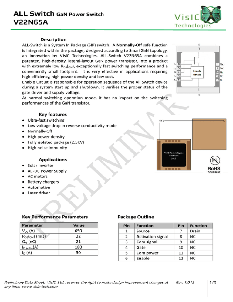
ALL-Switch is a System In Package (SIP) switch. A Normally-Off safe function
is integrated within the package, designed according to SmartGaN topology,
an innovation by VisIC Technologies. ALL-Switch V22N65A combines a
patented, high-density, lateral-layout GaN power transistor, into a product
with extremely low RDS(ON), exceptionally fast switching performance and a
conveniently small footprint. It is very effective in applications requiring
high efficiency, high power density and low cost.
Enable Circuit is responsible for operation sequence of the All Switch device
during a system start up and shutdown. It verifies the proper status of the
gate driver and supply voltage.
At normal switching operation mode, it has no impact on the switching
performances of the GaN transistor.
Key features
Ultra-fast switching
Low voltage drop in reverse conductivity mode
Normally-Off
High power density
Fully isolated package (2.5KV)
High noise immunity
Applications
Solar Inverter
AC-DC Power Supply
AC motors
Battery chargers
Automotive
Laser driver
Key Performance Parameters
Parameter
VDS (V)
RDS(ON) (mΩ)
QG (nC)
ID,pulse(A)
ID (A)
Value
650
22
21
180
50
Package Outline
Pin
1
2
3
4
5
6
Function
Source
Activation signal
Com signal
Gate
Com power
Enable
Preliminary Data Sheet: VisIC, Ltd. reserves the right to make design improvement changes at
any time. www.visic-tech.com
Pin
7
8
9
10
11
12
Function
Drain
NC
NC
NC
NC
NC
Rev. 1.012
/
1/9
ALL Switch GaN Power Switch
V22N65A
Maximum ratings (Tj =25ºC unless otherwise specified)
Values
Parameter
Symbol
Min Typical
Unit
Conditions
TC =25C
TC =100C
Max
Continuous drain current
ID
-
-
53
42
A
Pulsed drain current
ID,pulse
-
-
180
A
Gate source voltage
VGS
-20
-
0
V
Power dissipation
PTOT
-
-
278
W
Operating and storage
temperature
Tj ,Tstg
-55
-
+ 150
TC
-
-
+130
Continuous reverse current
Is
-
-
50
A
Reverse pulse current1)
Is,pulse
-
-
140
A
static
C
Thermal characteristics
Values
Parameter
Symbol
Min Typical
Unit
Conditions
Top cooling
via top
Thermal pad
Max
Thermal resistance, junction-case RθJC
-
-
0.45
C/W
Thermal resistance, junction ambient
RθJA
-
-
65
C/W
Soldering peak temperature
Tsold
-
-
260
C
from case for
10s
1) Duty cycle =10% limited by Tj
Preliminary Data Sheet: VisIC, Ltd. reserves the right to make design improvement changes at
any time. www.visic-tech.com
Rev. 1.012
/
2/9
ALL Switch GaN Power Switch
V22N65A
Electrical characteristics (Tj =25C unless otherwise specified)
Symbol
Values
Unit Conditions
Min Typical Max
Drain-source breakdown voltage
VDS
650
680
-
V
VGS= -15V 5)
Gate threshold voltage1)2)
V(GCs)th
-
5
-
V
Drain source leakage current1)
-
2
3
IDSS
VDCs= -VGCs ID=1mA
VGS= -15V
VDS= 650V5)Tj =25C
Parameter
Static
µA
-
75
200
Gate-source leakage current4)
IGSS
-
3
5
nA
Gate resistance
RG
-
0.7
-
Ω
-
22
24
-
42
46
-
-
2.40
-
-
2.65
-
-
0.2
-
-
0.4
Drain-source on state resistance
RDS(ON)
mΩ
Reverse voltage dropGaN non conductive
VR
Reverse voltage dropGaN conductive
VR
Reverse recovery time
trr
-
-
0
nS
Reverse recovery charge
Qrr
-
-
0
nC
Output Charge
Qoss
-
-
171
nC
Activation signal3)
Dynamic
Input capacitance
Output capacitance
Reverse transfer capacitance
Effective Output Capacitance, Energy
Related
Turn-on delay time
Fall time
Turn-off delay time
Rise time
V(As,En)
-
-15
-
V
Ciss
Coss
Crss
-
800
240
2.6
pF
-
760
200
1.3
CO(ER)
-
-
427
pF
td(on)
tf
td(off)
tr
-
7.5
5
36
2.5
-
ns
V
V
1) After applying Activation signal
2) Refer to -12V of pin 3
3) Device activation voltage to pin2 refer to pin3
4) GaN transistor
5) Short pin 1 to 3
Preliminary Data Sheet: VisIC, Ltd. reserves the right to make design improvement changes at
any time. www.visic-tech.com
VGS= -15V VDS= 650V5)
Tj =150C
VDS= 0V
VGS= -20V
f =1Mhz
VGS=0v ID=35A
Tj =25C
VGS=0v ID=35A
Tj =150C
ID=10A Tj =25C
ID=10A Tj =150C
ID=10A Tj =25C
ID=10A Tj =150C
VGS=-15v
VDS=400v
f=1MHz
VGS=-15V
VDS=400V
VGS=-15v
VDS=0 to 400V
VDS=400V
VGS=-15V
RG=2 Ω
ID=35A
Rev. 1.012
/
3/9
ALL Switch GaN Power Switch
V22N65A
Electrical characteristics (Tc =25ºC unless otherwise specified)
Parameter
Symbol
Values
Min Typical Max
Unit Conditions
Gate charge characteristics
Gate to source charge1)
Gate to drain charge
1)
Total gate charge1)
Gate plateau voltage
1)2)
QGS
-
3.2
-
QGD
-
12
-
QG
-
21
-
Vplateau
6
-
6.8
V
CC
-
20
-
pF
nC
VGS2)=0Vto 10V
VDS=400V ID=30A pulsed
Case to drain Capacitance
Capacitance
@ 1 MHz 1V RMS
1. After applying Activation signal
2. VGS is relative to -15V
Pin Characteristics
Parameter
Symbol
Pin 2 Activation signal (ref. to pin 3)
Disable ALL Switch = open
Pin 2
Enable voltage
Pin 2
Pin 3 Com signal (ref. to pin 1)
Voltage at disable mode
Pin 3
Voltage at Enable mode
Pin 3
Pin 4 Gate (Driver RTN at pin 5)
Gate Voltage for non-Conducting mode Pin 4
Gate Voltage for conducting mode
Pin 4
Pin 5 Com Power RTN for Driver (ref. to pin 3)
Disable voltage
Pin 5
Enable voltage
Pin 5
Pin 6 Enable (ref. to pin 3)
Enable voltage
Pin 6
Disable voltage (open)
Pin 6
Values
Unit Conditions
Min Typical Max
10V
-4
0
-15
-1.5
-20
V
0
0
7
0
8
0.1
V
-7
-3
-8
0
-20
0
0.3
0
0.5
0.1
0.6
0.1
V
-4
0
-15
0
-20
0.1
V
Preliminary Data Sheet: VisIC, Ltd. reserves the right to make design improvement changes at
any time. www.visic-tech.com
V
VDS=400V
VDS=400V
VDS=400V
VDS=400V
VDS=400V
Rev. 1.012
/
4/9
ALL Switch GaN Power Switch
V22N65A
Package Outlines
Preliminary Data Sheet: VisIC, Ltd. reserves the right to make design improvement changes at
any time. www.visic-tech.com
Rev. 1.012
/
5/9
ALL Switch GaN Power Switch
V22N65A
Typical Operating Circuit
Note: A voltage threshold gap V>2V between Driver UVLO and VRef is needed for safe operation.
VUVLO> VRef >Vth
Preliminary Data Sheet: VisIC, Ltd. reserves the right to make design improvement changes at
any time. www.visic-tech.com
Rev. 1.012
/
6/9
ALL Switch GaN Power Switch
V22N65A
Electrical characteristics diagrams
Figure 1: Power dissipation
Figure 3: Gate charge
Figure 2: Drain-source on-state resistance
Figure 4:Typical capacitances
Preliminary Data Sheet: VisIC, Ltd. reserves the right to make design improvement changes at
any time. www.visic-tech.com
Rev. 1.012
/
7/9
ALL Switch GaN Power Switch
V22N65A
Figure 5: Typical Coss stored energy
Figure 6: Switching Energy vs Drain Current
1)
Circuit Used to Determine Switching Energy
Figure 7: Reverse conductivity
Preliminary Data Sheet: VisIC, Ltd. reserves the right to make design improvement changes at
any time. www.visic-tech.com
Rev. 1.012
/
8/9
1
ALL Switch GaN Power Switch
V22N65A
Important Notice – VisIC Technologies reserve the right to make corrections, enhancements, improvements and
other changes to its semiconductor products, latest issue, and to discontinue any product. Buyers should obtain the
latest relevant information before placing orders and should verify that such information is current and complete.
Unless expressly approved in writing by an authorized representative of VisIC technologies , VisIC technologies
components are not designed or tested for use in, and is not intended for use in applications in which failure of the
product could lead to death, personal injury or property damage, including but not limited to equipment used in the
operation of nuclear facilities, life-support machines, cardiac defibrillators or similar emergency medical equipment,
aircraft navigation or communication or control systems, air traffic control systems, weapons systems, authorized or
warranted for use in lifesaving, life sustaining, military, or space applications, nor in products or systems where failure
or malfunction may result in personal injury, death, or property or environmental damage. The information given in
this document shall not in any event be regarded as a guarantee of performance. VisIC Technologies hereby disclaims
any or all warranties and liabilities of any kind, including but not limited to warranties of non-infringement of
intellectual property rights. All other brand and product names are trademarks or registered trademarks of their
respective owners. Information provided herein is intended as a guide only and is subject to change without notice.
The information contained herein or any use of such information does not grant, explicitly, or implicitly, to any party
any patent rights, licenses, or any other intellectual property rights. All rights reserved.
Preliminary Data Sheet: VisIC, Ltd. reserves the right to make design improvement changes at
any time. www.visic-tech.com
Rev. 1.012
/
9/9

