High-Power Photodetectors
advertisement
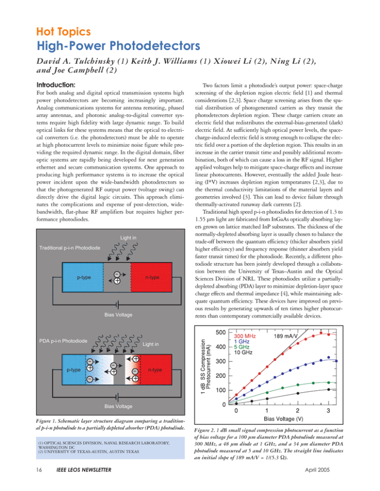
Hot Topics High-Power Photodetectors David A. Tulchinsky (1) Keith J. Williams (1) Xiowei Li (2), Ning Li (2), and Joe Campbell (2) Introduction: For both analog and digital optical transmission systems high power photodetectors are becoming increasingly important. Analog communications systems for antenna remoting, phased array antennas, and photonic analog-to-digital converter systems require high fidelity with large dynamic range. To build optical links for these systems means that the optical to electrical converters (i.e. the photodetectors) must be able to operate at high photocurrent levels to minimize noise figure while providing the required dynamic range. In the digital domain, fiber optic systems are rapidly being developed for next generation ethernet and secure communication systems. One approach to producing high performance systems is to increase the optical power incident upon the wide-bandwidth photodetectors so that the photogenerated RF output power (voltage swing) can directly drive the digital logic circuits. This approach eliminates the complications and expense of post-detection, widebandwidth, flat-phase RF amplifiers but requires higher performance photodiodes. Light in Traditional p-i-n Photodiode – + p-type n-type Bias Voltage PDA p-i-n Photodiode p-type Two factors limit a photodiode’s output power: space-charge screening of the depletion region electric field [1] and thermal considerations [2,3]. Space charge screening arises from the spatial distribution of photogenerated carriers as they transit the photodetectors depletion region. These charge carriers create an electric field that redistributes the external-bias-generated (dark) electric field. At sufficiently high optical power levels, the spacecharge-induced electric field is strong enough to collapse the electric field over a portion of the depletion region. This results in an increase in the carrier transit time and possibly additional recombination, both of which can cause a loss in the RF signal. Higher applied voltages help to mitigate space-charge effects and increase linear photocurrents. However, eventually the added Joule heating (I*V) increases depletion region temperatures [2,3], due to the thermal conductivity limitations of the material layers and geometries involved [3]. This can lead to device failure through thermally-activated runaway dark currents [2]. Traditional high speed p-i-n photodiodes for detection of 1.3 to 1.55 µm light are fabricated from InGaAs optically absorbing layers grown on lattice matched InP substrates. The thickness of the normally-depleted absorbing layer is usually chosen to balance the trade-off between the quantum efficiency (thicker absorbers yield higher efficiency) and frequency response (thinner absorbers yield faster transit times) for the photodiode. Recently, a different photodiode structure has been jointly developed through a collaboration between the University of Texas–Austin and the Optical Sciences Division of NRL. These photodiodes utilize a partiallydepleted absorbing (PDA) layer to minimize depletion-layer space charge effects and thermal impedance [4], while maintaining adequate quantum efficiency. These devices have improved on previous results by generating upwards of ten times higher photocurrents than contemporary commercially available devices. Light in – + – – + + – + n-type Bias Voltage Figure 1. Schematic layer structure diagram comparing a traditional p-i-n photodiode to a partially depleted absorber (PDA) photodiode. (1) OPTICAL SCIENCES DIVISION, NAVAL RESEARCH LABORATORY, WASHINGTON DC (2) UNIVERSITY OF TEXAS-AUSTIN, AUSTIN TEXAS 16 IEEE LEOS NEWSLETTER Figure 2. 1 dB small signal compression photocurrent as a function of bias voltage for a 100 µm diameter PDA photodiode measured at 300 MHz, a 48 µm diode at 1 GHz, and a 34 µm diameter PDA photodiode measured at 5 and 10 GHz. The straight line indicates an initial slope of 189 mA/V = 1/(5.3 Ω). April 2005 Partially Depleted Absorber (PDA) Photodiodes: Figure 1 shows the structure of a conventional p-i-n and a PDA photodiode. In a conventional semiconductor p-i-n photodiode, incident light generates electron-hole pairs in a fully-depleted intrinsic region. Once generated, each carrier drifts in opposite directions towards their respective contact layers. A space-chargeinduced electric field arises from the separation of these electronhole pairs. Space-charge effects can be minimized by decreasing the depletion layer thickness (d) since this decreases the total depletion region charge density. An additional and equally beneficial effect of having a thin depletion layer is the increased electric field that results from the same externally applied voltage (E=V/d). This allows for a reduction in the applied bias voltage which results in less Joule heating of the depletion region at similar photocurrents. However, thinning the optically-absorbing depletion layer has the deleterious effect of lowering the optical responsivity. To compensate for this, PDA photodiodes include p-type and/or n-type doped absorbers adjacent to the depletion region. With this design, the pdoped absorber injects electrons into the depletion region while the n-doped absorber injects holes. These minority carriers in the doped absorbers move through a combination of both drift and diffusion. The drift component of transport arises from the small electric field generated as a result of the current flow ( J = σ E). This term, being current dependent, causes the bandwidth in these devices to increase slightly [4] with increasing current. This characteristic can be minimized in the PDA photodiode by utilizing a graded doping of the optically absorbing regions on either side of the intrinsic layer to increase transport via a small built-in quasi-electric field. decrease to near zero (i.e. clipping behavior). At higher applied voltages clipping is reduced and the output RF power exceeds +25 dBm until it begins to saturate above 6 V bias. When amplitude modulated light is incident upon a 34 µm diameter photodiode, 130 mA of photocurrent is able to generate upwards of +24.5 dBm at 2 GHz and +23.5 dBm at 6 GHz of RF power into a 50 Ω load. These are the highest reported output RF powers directly generated from a photodetector. Summary: In conclusion, we have described high-saturation-current, widebandwidth photodiodes. The partially-depleted-absorber photodiode has achieved record high current (bandwidth) outputs of 500mA (300MHz), 325mA (1 GHz), 150mA (5GHz), and 105mA (10GHz). The maximum RF output power generated from these partially-depleted-absorber photodiodes exceeds +23.5 dBm from DC to 6 GHz. Acknowledgements: This work supported in part by DARPA. Performance Results: Figure 2 shows a summary of the 1-dB small-signal compression photocurrents as a function of bias voltage at several different RF frequencies. The 1-dB small-signal compression photocurrent is quantified by measuring a 1 dB (20%) drop in RF signal response at a specified frequency while a separate continuous wave (CW) unmodulated optical signal is applied to the photodiode. For a 100 µm diameter diode, measured at 300 MHz, the peak 1-dB smallsignal compression photocurrent observed was 500 mA. Performance reduces to 325 mA at 1 GHz (48 µm diameter), 150 mA at 5 GHz (34 µm diameter) and 105 mA at 10 GHz (34 µm diameter). These photocurrents are five to ten times higher than commercially available detectors at these frequencies. For the case of the 100 µm diode, the initial slope of the compression current with applied voltage fits a straight line with a slope of ~189 mA/V. This initial slope is characteristic of a reversed bias series resistance of 5.3 Ω. We believe the extremely large photocurrents generated by these detectors are a direct result of the low series resistance of these photodiodes. Above a bias of 1-2 Volts, other factors limit the photocurrent. Figure 3 shows the RF power generated by a 100 MHz 100% amplitude modulation depth, 150 mW optical beam incident on a 100 µm diameter PDA photodiode with a fixed average photocurrent of 130 mA as a function of applied voltage. At low applied voltages, the external bias limits the possible output voltage swing (and maximum output RF power) due to the large signal I*R loading from the output impedance. This condition causes the photodiode terminal voltage to April 2005 Figure 3. Peak RF power generated from a 100 % amplitude modulation depth optical source as a function of bias voltage from a 100 µm diameter PDA photodiode at 100 MHz and from a 34 µm diameter PDA photodiode at 2 and 6 GHz. References: 1. K.J. Williams, R.D. Esman, and M. Dagenais, “Effects of High Space-Charge Fields on the Response of Microwave Photodetectors,” IEEE Photon. Tech. Lett., vol. 6, no. 5, pp. 639641, 1994. 2. J. Paslaski, P.C. Chen, J.S. Chen, C.M. Gee, and N. Bar-Chaim, “High-Power Microwave Photodiode for Improving Performance of RF Fiber Optic Links,” Proc. SPIE, Photonics and Radio Frequency, Vol. 2844, 1996 Denver CO, pp. 110-119. 3. K. J. Williams and R. D. Esman, “Design Considerations for High Current Photodetectors,” Journal of Lightwave Technology, 17, pp 1443-1454, (1999). 4. D. A. Tulchinsky, X. LI, N. Li, S. Demiguel, J. C. Campbell, and K. J. Williams, “High-Saturation Current Wide-Bandwidth Photodetectors,” IEEE Journal of Selected Topics in Quantum Electronics, 10, 702-708 (2004). IEEE LEOS NEWSLETTER 17
