OP220
Dual Micropower
Operational Amplifier
V+
OUT A
-IN A
+IN A
V-
OP220
OUT B
-IN B
+IN B
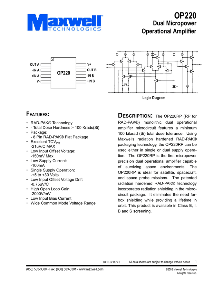
Logic Diagram
DESCRIPTION:
• RAD-PAK® Technology
• - Total Dose Hardness > 100 Krads(Si)
• Package:
- 8 Pin RAD-PAK® Flat Package
• Excellent TCVOS
-21uV/C MAX
• Low Input Offset Voltage:
-150mV Max
• Low Supply Current:
-100mA
• Single Supply Operation:
-+5 to +30 Volts
• Low Input Offset Voltage Drift
-0.75uV/C
• High Open Loop Gain:
-2000V/mV
• Low Input Bias Current
• Wide Common Mode Voltage Range
RAD-PAK®) monolithic dual operational
amplifier microcircuit features a minimum
100 kilorad (Si) total dose tolerance. Using
Maxwells radiation hardened RAD-PAK®
packaging technology, the OP220RP can be
used either in single or dual supply operation. The OP220RP is the first micropower
precision dual operational amplifier capable
of surviving space environments. The
OP220RP is ideal for satellite, spacecraft,
and space probe missions. The patented
radiation hardened RAD-PAK® technology
incorporates radiation shielding in the microcircuit package. It eliminates the need forbox shielding while providing a lifetime in
orbit. This product is available in Class E, I,
B and S screening.
08.15.02 REV 3
(858) 503-3300 - Fax: (858) 503-3301 - www.maxwell.com
The OP220RP (RP for
All data sheets are subject to change without notice
1
©2002 Maxwell Technologies
All rights reserved.
Memory
FEATURES:
OP220
Dual Micropower Operational Amplifier
TABLE 1. OP220 PINOUT DESCRIPTION
PIN
SYMBOL
DESCRIPTION
1
Out A
Output Amplifier A
2
-IN A
Inverting Input Amplifier A
3
+ IN A
Non-Inverting Input Amplifier A
4
-V
Negative Supply Voltage
5
+ IN B
Non-Inverting Input Amplifier B
6
-IN B
Inverting Input Amplifier B
7
Out B
Output Amplifier B
8
+V
Positive Supply Voltage
TABLE 2. OP220 ABSOLUTE MAXIMUM RATINGS
SYMBOL
MIN
MAX
UNIT
Supply Voltage
--
±18
V
Differential Input Voltage
--
30
V
--
Supply
Voltage
V
500
mW
Input Voltage
VI
Output Short-Circuit Duration
Memory
PARAMETER
Indefinate
Power Dissipation
PD
Storage Temperature Range
TS
-65
150
°C
Operating Temperature Range
TA
-55
125
°C
TABLE 3. DELTA LIMITS
PARAMETER
VARIATION
ISY
±10% of specified value in Table 4
TABLE 4. OP220 ELECTRICAL CHARACTERISTICS
(VS=± 2.5V TO ±15V, TA = -55 TO +125°C, UNLESS OTHERWISE SPECIFIED)
PARAMETER
Supply Current
Both Amplifiers
SYMBOL
ISY
TEST CONDITIONS
Vs = ±2.5 V, No Load
Vs = ±15 V, No Load
Common-Mode Rejection Ratio
CMRR
Vs = ±15V
TA = 25°C
Power Supply Rejection Ratio
PSRR
Vs = ±2.5V TO Vs = ±15V
TA = 25°C
08.15.02 REV 3
SUBGROUPS
MIN
TYP
MAX
UNITS
1, 2, 3
---
135
190
170
250
uA
4
90
100
1, 2, 3
--
6
dB
18
uV/V
All data sheets are subject to change without notice
2
©2002 Maxwell Technologies
All rights reserved.
OP220
Dual Micropower Operational Amplifier
TABLE 4. OP220 ELECTRICAL CHARACTERISTICS
(VS=± 2.5V TO ±15V, TA = -55 TO +125°C, UNLESS OTHERWISE SPECIFIED)
PARAMETER
Input Offset Voltage
Input Offset Voltage Drift
Input Offset Current
SYMBOL
TEST CONDITIONS
SUBGROUPS
MIN
TYP
MAX
UNITS
VOS
VS = ±15V
1, 2, 3
120
300
uV
TCVOS
VS = ±15V
1, 2, 3
0.75
--
uV/°C
VCM = 0
1, 2, 3
---
0.5
2
nA
RS = 0Ω
1, 2, 3
---
10
--
pA/°C
12
20
nA
13.2
V
IOS
Input Offset Current Drift
Input Bias Current
IB
VCM = 0
1, 2, 3
---
Input Common-Mode
Voltage Range
IVR
Vs = ±15V
1, 2, 3
-15
Large Signal Voltage Gain
AVO
Vs = ±15V
VO = ±10V
RL = 50KΩ
1, 2, 3
500
1000
Output Voltage Swing
VO
VS = ±15V, RL = 50KΩ
1, 2, 3
-13.8
--
V/mV
13.8
V
Memory
Typical Performance Characteristics
08.15.02 REV 3
All data sheets are subject to change without notice
3
©2002 Maxwell Technologies
All rights reserved.
Dual Micropower Operational Amplifier
OP220
Typical Performance Characteristics
Memory
08.15.02 REV 3
All data sheets are subject to change without notice
4
©2002 Maxwell Technologies
All rights reserved.
OP220
Dual Micropower Operational Amplifier
Memory
8-PIN RAK-PAK® FLAT PACKAGE
SYMBOL
DIMENSION
MIN
NOM
MAX
A
0.119
0.132
0.149
b
0.010
0.017
0.022
c
0.004
0.005
0.009
D
0.250
0.255
0.260
E
0.250
0.255
0.260
E1
--
--
0.290
E2
0.125
0.145
0.150
E3
0.045
0.055
--
e
0.050 BSC
L
0.338
0.348
0.358
Q
0.021
0.025
0.045
S1
0.005
0.019
--
N
8
F8-01
Note: All dimensions in inches.
08.15.02 REV 3
All data sheets are subject to change without notice
5
©2002 Maxwell Technologies
All rights reserved.
Dual Micropower Operational Amplifier
OP220
Important Notice:
These data sheets are created using the chip manufacturer’s published specifications. Maxwell
Technologies verifies functionality by testing key parameters either by 100% testing, sample testing or characterization.
The specifications presented within these data sheets represent the latest and most accurate
information available to date. However, these specifications are subject to change without notice
and Maxwell Technologies assumes no responsibility for the use of this information.
Maxwell Technologies’ products are not authorized for use as critical components in life support
devices or systems without express written approval from Maxwell Technologies.
Any claim against Maxwell Technologies must be made within 90 days from the date of shipment
from Maxwell Technologies. Maxwell Technologies’ liability shall be limited to replacement of
defective parts.
Memory
08.15.02 REV 3
All data sheets are subject to change without notice
6
©2002 Maxwell Technologies
All rights reserved.
OP220
Dual Micropower Operational Amplifier
Product Ordering Options
Model Number
OP220
RP
F
X
Option Details
Feature
Monolithic
S = Maxwell Class S
B = Maxwell Class B
I = Industrial (testing @ -55°C,
+25°C, +125°C)
E = Engineering (testing @ +25°C)
Package
F = Flat Pack
Radiation Feature
RP = RAD-PAK® package
Base Product
Nomenclature
Low-Power Quad Operational
Amplifier
08.15.02 REV 3
All data sheets are subject to change without notice
Memory
Screening Flow
7
©2002 Maxwell Technologies
All rights reserved.


