AMMC-6530
5–30 GHz Image Reject Mixer
Vg
Data Sheet
drain
IF1
IF2
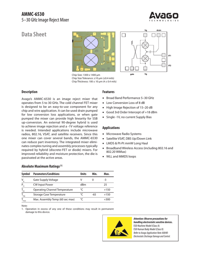
Chip Size: 1300 x 1400 µm
Chip Size Tolerance: ±10 µm (±0.4 mils)
Chip Thickness: 100 ± 10 µm (4 ± 0.4 mils)
Description
Features
Avago’s AMMC-6530 is an image reject mixer that
­operates from 5 to 30 GHz. The cold channel FET mixer
is designed to be an easy-to-use component for any
chip and wire application. It can be used drain pumped
for low conversion loss applications, or when gate
pumped the mixer can provide high linearity for SSB
up‑conversion. An external 90‑degree hybrid is used
to achieve image rejection and a -1V voltage ­reference
is needed. Intended applications include ­ microwave
radios, 802.16, VSAT, and satellite receivers. Since this
one mixer can cover several bands, the AMMC-6530
can reduce part inventory. The ­integrated mixer eliminates complex tuning and ­assembly ­processes typically
required by hybrid (discrete-FET or diode) mixers. For
improved reliability and moisture protection, the die is
passivated at the active areas.
•
•
•
•
•
gate
Vg
Broad Band Performance 5–30 GHz
Low Conversion Loss of 8 dB
High Image Rejection of 15–20 dB
Good 3rd Order Intercept of +18 dBm
Single -1V, no current Supply Bias
Applications
•
•
•
•
Microwave Radio Systems
Satellite VSAT, DBS Up/Down Link
LMDS & Pt-Pt mmW Long Haul
Broadband Wireless Access (including 802.16 and
802.20 WiMax)
• WLL and MMDS loops
Absolute Maximum Ratings [1]
Symbol Parameters/Conditions
Units
Min.
Max.
Vg
Gate Supply Voltage
V
0
-3
Pin
CW Input Power
dBm
25
Tch
Operating Channel Temperature
°C
+150
Tstg
Storage Case Temperature
°C
+150
Tmax
Max. Assembly Temp (60 sec max)
°C
-65
+300
Note:
1. Operation in excess of any one of these conditions may result in permanent
damage to this device.
Attention: Observe precautions for
handling electrostatic ­sensitive devices.
ESD Machine Model (Class A)
ESD Human Body Model (Class 0)
Refer to Avago Application Note A004R:
Electrostatic Discharge Damage and Control.
AMMC-6530 DC Specifications/Physical Properties[1]
Symbol
Parameters and Test Conditions
Units
Typ.
Ig
Gate Supply Current (under any RF power drive and temperature)
mA
0
Vg
Gate Supply Operating Voltage
V
-1V
Note:
1. Ambient operational temperature TA=25°C unless otherwise noted.
AMMC-6530 Typical Performance[2, 3] (TA = 25°C, Vg= -1V, IF frequency = 1 GHz, Zo=50 Ω)
Symbol
Parameters and Test Conditions
Units
Gate Pumped
Drain Pumped
FRF
RF Frequency Range
GHz
5 – 30
5 – 30
FLO
LO Frequency Range
GHz
5 – 30
5 – 30
FIF
IF Frequency Range
GHz
DC – 5
DC – 5
Down Conversion
Up Conversion
Down Conversion
PLO
LO Port Pumping Power
dBm
>10
>0
>10
CG
RF to IF Conversion Gain
dB
-10
-15
-8
RL_RF
RF Port Return Loss
dB
5
5
10
RL_LO
LO Port Return Loss
dB
10
10
5
RL_IF
IF Port Return Loss
dB
10
10
10
IR
Image Rejection Ratio
dB
15
15
15
LO-RF Iso.
LO to RF Port Isolation
dB
22
25
22
LO-IF Iso.
LO to IF Port Isolation
dB
25
25
25
RF-IF Iso.
RF to IF Port Isolation
dB
15
15
15
IIP3
Input IP3, Fdelta=100 MHz, Prf = -10 dBm, Plo = 15 dBm
dBm
18
—
10
P-1
Input Port Power at 1dB gain compression point, Plo=+10 dBm
dBm
8
—
0
NF
Noise Figure
dB
10
—
12
Notes:
2. Small/Large signal data measured in a fully de-embedded test fixture form TA = 25°C.
3. Specifications are derived from measurements in a 50Ω test environment.
AMMC-6530 RF Specifications in Drain Pumped Test Configuration[4, 5, 6]
(TA = 25°C, Vg = -1.0V, PLO = +10 dBm, Zo =50 Ω)
Symbol
Parameters and Test Conditions
CG
Conversion Gain
IR
f = 7 GHz
f = 18 GHz
f = 28 GHz
Image Rejection Ratio
Units
Min
Typ.
dB
dB
dB
-12.0
-10.0
-12.5
-10.5
-8.0
-10.0
dB
-23.5
Max
-18
Notes:
4. Performance verified 100% on-wafer.
5. 100% on-wafer RF testing is done at RF frequency = 7, 18, and 28 GHz; IF frequency = 2 GHz.
6. The external 90 degree hybrid coupler is from M/A-COM: PN 2032-6344-00. Frequency 1.0 –
2.0 GHz.
AMMC-6530 Typical Performance under Gate Pumped Down Conversion Operation
(TA = 25°C, Vg = -1V, Z o = 50Ω)
RF
Vg
drain
LSB
IF1
IF2
USB
gate
Vg
Note: The external 90° hybrid coupler is from M/ACOM: PN 2032-6344-00. Frequency is 1.0 – 2.0 GHz.
-1V
LO
0
-5
-10
-10
-15
-20
-25
-30
-35
-40
-50
5
10
15
20
25
-15
-20
-25
-30
-35
-50
5
10
20
25
15
20
10
20
FREQUENCY (GHz)
Figure 4. Noise Figure.
LO=+7 dBm, IF=1 GHz.
25
30
15
5
15
20
25
30
0
5
10
15
20
25
FREQUENCY (GHz)
Figure 5. Input 3rd Order Intercept Point.
IF=1 GHz.
-5
-10
-15
-20
Plo=15(dBm)
Plo=10(dBm)
15
10
Figure 3. RF Port Input Power P-1dB.
LO=+10 dBm, IF=1 GHz.
10
5
10
5
FREQUENCY (GHz)
CONVERSION GAIN (dB)
25
IIP3 (dBm)
20
5
-5
30
Figure 2. Conversion Gain with IF
terminated for Low Side Conversion
LO=+10 dBm, IF=1 GHz.
Figure 1. Conversion Gain with IF
terminated for High Side Conversion
LO=+10 dBm, IF=1 GHz.
NOISE FIGURE (dB)
15
FREQUENCY (GHz)
FREQUENCY (GHz)
0
5
USB(dB)
LSB(dB)
-45
30
10
0
-40
USB(dB)
LSB(dB)
-45
15
INPUT POWER (dB)
0
-5
CONVERSION GAIN (dB)
CONVERSION GAIN (dB)
Highly linear down conversion or up conversion mixer application (Gate pumped mixer operation)
30
-25
-10
-5
0
5
10
15
LO POWER (dBm)
Figure 6. Conversion Gain vs. LO Power.
RF=21 GHz (-20 dBm), LO=20 GHz.
20
AMMC-6530 Typical Performance under Gate Pumped Down Conversion ­Operation
(TA = 25°C, Vg = -1V, Z o=50Ω)
0
CONVERSION GAIN (dB)
CONVERSION GAIN (dB),
RETURN LOSS (dB)
0
-5
-10
-15
-5
-10
-15
Conv. Gain (dB)
Return Loss (dB)
-20
0
1
2
3
4
5
-20
-2
6
-1.5
FREQUENCY (GHz)
Figure 7. Conversion Gain and Match vs.
IF Frequency. RF=20 GHz, LO=10 dBm.
60
RF
LO
50
ISOLATION (dB)
-5
-10
40
30
20
-15
RF-IF
LO-IF
LO-RF
10
-20
0
5
10
15
20
25
30
FREQUENCY (GHz)
Figure 9. RF & LO Return Loss. LO=10 dBm.
-0.5
Figure 8. Conversion Gain vs. Gate Voltage.
RF=20 GHz, LO=10 dBm.
0
RETURN LOSS (dB)
-1
Vg (V)
0
5
10
15
20
25
30
FREQUENCY (GHz)
Figure 10. Isolation. LO=+10 dBm, IF=1 GHz.
AMMC-6530 Typical Performance under Gate Pumped Up Conversion ­Operation
(TA = 25°C, Vg = -1V, Z o=50Ω)
LO
-1V
Vg
gate
LSB
IF2
IF1
USB
drain
Vg
RF
0
0
USB (dB)
LSB (dB)
-10
-15
-20
-25
-30
-35
-10
-15
-20
-25
-30
-35
-40
-40
-45
-45
-50
5
10
15
USB (dB)
LSB (dB)
-5
CONVERSION GAIN (dB)
CONVERSION GAIN (dB)
-5
20
25
-50
30
5
10
15
20
25
30
FREQUENCY (GHz)
FREQUENCY (GHz)
Figure 12. Up-conversion Gain wth IF
terminated for High Side Conversion.
LO=+5 dBm, IF=+5 dBm, IF=1 GHz.
Figure 11. Up-conversion Gain with IF
terminated for Low Side Conversion.
LO=+5 dBm, IF=+5 dBm, IF=1 GHz.
0
-5
CONVERSION LOSS (dB)
-5
ISOLATION (dB)
-10
-15
-20
-25
-30
-7
-9
-11
-13
-35
-40
5
10
15
20
25
30
FREQUENCY (GHz)
Figure 13. LO-RF Up-conversion Isolation.
-15
0
2
4
6
8
10 12 14 16 18 20
PLO=PIF (dB)
Figure 14. Up-conversion Gain vs. Pumping
Power. LO power=IF power, IF=1 GHz,
RF=25 GHz.
AMMC-6530 Typical Performance under Drain Pumped Down Conversion Operation
(TA = 25°C, Vg = -1V, Z o = 50Ω)
LO
Vg
drain
USB
IF1
IF2
LSB
gate
Vg
Note: The external 90° hybrid coupler is from M/ACOM: PN 2032-6344-00. Frequency is 1.0 – 2.0 GHz.
RF
-1V
0
-5
-10
-10
-15
-20
-25
-30
-35
-40
-50
5
10
15
20
25
-15
-20
-25
-30
-35
-50
5
USB(dBm)
LSB(dBm)
-45
30
10
0
-40
USB (dB)
LSB (dB)
-45
15
INPUT POWER (dBm)
0
-5
CONVERSION GAIN (dB)
CONVERSION GAIN (dB)
Low conversion loss mixer configuration (Drain pumped mixer operation)
5
10
FREQUENCY (GHz)
15
20
25
-5
30
5
10
FREQUENCY (GHz)
Figure 15. Conversion Gain with IF
terminated for Low Side Conversion.
LO=+10 dBm, IF=1 GHz.
Figure 16. Conversion Gain with IF
terminated for High Side Conversion.
LO=+10 dBm, IF=1 GHz.
20
25
30
Figure 17. RF Port Input Power P-1dB.
LO=+10 dBm, IF=1 GHz.
25
20
15
FREQUENCY (GHz)
0
10
5
0
15
10
5
10
15
20
25
30
Figure 18. Noise Figure. LO=+7 dBm, IF=1 GHz.
0
-5
-10
-15
-20
5
FREQUENCY (GHz)
CONVERSION GAIN (dB)
20
15
IIP3 (dBm)
NOISE FIGURE (dB)
Plo=10(dBm)
Plo=15(dBm)
5
10
15
20
25
30
Flo (dB)
Figure 19. Input 3rd Order Intercept Point.
IF=1 GHz.
-25
-10
-5
0
5
10
15
20
LO POWER (dBm)
Figure 20. Conversion Gain vs. LO power.
RF=21 GHz (-20 dBm), LO=20 GHz.
Biasing and Operation
The recommended DC bias condition for optimum
­performance, and reliability is Vg = -1 volts. This can
be applied to either of the two Vg connections as they
are internally connected. There is no current consumption for the gate biasing because the FET mixer was
designed for passive operation. For down conversion,
the AMMC‑6530 may be configured in a low loss or high
linearity application. In a low loss configuration, the
LO is applied through the drain. In this configuration,
the AMMC-6530 is a “drain pumped mixer”. For higher
linearity applications, the LO is applied through the gate.
In this configuration, the AMMC-6530 is a “gate pumped
mixer” (or Resistive mixer). The mixer is also suitable for
up-conversion applications under the gate pumped
mixer operation shown on page 5.
Please note that the image rejection and isolation performance is dependent on the selection of the low
frequency quadrature hybrid. The performance specification of the low frequency quadrature hybrid as well
as the phase balance and VSWR of the interface to the
AMMC-6530 will affect the overall mixer performance.
Figure 21. Simplified MMIC Schematic.
Assembly Techniques
The backside of the MMIC chip is RF ground. For microstrip applications the chip should be attached directly
to the ground plane (e.g. circuit carrier or heatsink) using
electrically conductive epoxy [1, 2].
For best performance, the topside of the MMIC should be
brought up to the same height as the circuit surrounding it. This can be accomplished by mounting a gold
plate metal shim (same length and width as the MMIC)
under the chip which is of correct thickness to make the
chip and adjacent circuit the same height. The amount of
epoxy used for the chip and/or shim attachment should
be just enough to provide a thin fillet around the bottom
perimeter of the chip or shim. The ground plane should
be free of any residue that may jeopardize electrical or
mechanical attachment.
The location of the RF bond pads is shown in Figure
Figure 22. AMMC-6530 Bond Pad locations.
23. Note that all the RF input and output ports are in a
Ground-Signal-Ground configuration.
The chip is 100 µm thick and should be handled with
care.
RF connections should be kept as short as reasonable
to minimize performance degradation due to undesirable series inductance. A single bond wire is normally
sufficient for signal connections, however double
bonding with 0.7 mil gold wire or use of gold mesh is
recommended for best performance, especially near the
high end of the frequency band. Thermosonic wedge
bonding is the preferred method for wire attachment to
the bond pads.
This MMIC has exposed air bridges on the top surface
and should be handled by the edges or with a custom
collet (do not pick up the die with a vacuum on die
center).
Gold mesh can be attached using a 2 mil round tracking
tool and a tool force of approximately 22 grams and a
ultrasonic power of roughly 55 dB for a duration of 76±8
mS. The guided wedge at an untrasonic power level of
64 dB can be used for 0.7 mil wire. The recommended
wire bond stage temperature is 150±2°C. Caution should
be taken to not exceed the Absolute Maximum Rating
for assembly temperature and time.
This MMIC is also static sensitive and ESD precautions
should be taken.
Notes:
1. Ablebond 84-1 LM1 silver epoxy is recommended.
2. Eutectic attach is not recommended and may jeopardize reliability
of the device.
Part Number Ordering Information
Part Number
Devices per Container
AMMC-6530-W10
10
AMMC-6530-W50
50
Gnd
IF1
LO/RF
IF2
Vg
RF/LO
Figure 23. AMMC-6530 Assembly Diagram.
For product information and a complete list of distributors, please go to our web site:
www.avagotech.com
Avago, Avago Technologies, and the A logo are trademarks of Avago Technologies in the United States and other countries.
Data subject to change. Copyright © 2005-2008 Avago Technologies. All rights reserved. Obsoletes 5989-3945EN
AV02-1293EN - July 30, 2008


