HV Waveform Development Tool
Features
• GUI interface under Windows
− Drive scheme editor
− Waveform editor
− Import of Bitmap
− Energy calculation
• Hardware Driver Kit
− RS232 interface
− Fast speed connector for display
− Possibility for external voltage sources
• Powered by Alpha3D driver chip
− 1/16 VGA waveform generator
− 7 HV row levels + gnd
− 5 HV col levels +gnd
− gnd to 100V line drive
− 4-bit PWM gray levels for columns
− 12 integrated 3.0V → 100 V generators
⇒ Maximum flexibility in waveform synthesis!!
Description
The Waveform Development Tool addresses the unique needs of “non-volatile reflective display systems”-developers. It
consists of a 120X160 output waveform generator, based on our special developed Alpha3D chip, and a user-friendly
GUI under Windows©. Intended for developing and prototyping different types of high-voltage display systems, it features maximum flexibility in waveform synthesis in order to achieve maximum optical performance at minimum power
consumption.
The GUI interface under Windows©
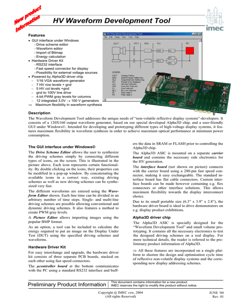
The Drive Scheme Editor allows the user to synthesize
the driving schemes simply by connecting different
types of icons, on the screen. This is illustrated in the
picture above. Each icon represents certain functionality. By double clicking on the icons, their properties can
be modified in a pop-up window. By concatenating the
available icons in a correct way, existing driving
schemes as well as new driving schemes can be synthesized very fast.
The different waveforms are entered using the Waveform Editor shown. Each line time can be divided in an
arbitrary number of time steps. Single- and multi-line
driving schemes are possible allowing conventional and
dynamic driving schemes. It also features a method to
create PWM gray levels.
A Picture Editor allows importing images using the
popular BMP format.
As an option, a tool can be included to calculate the
energy required to put an image on the Display Under
Test (DUT) using the specified driving schemes and
waveforms.
Hardware Driver Kit
For easy interchange and upgrade, the hardware driver
kit consists of three separate PCB boards, stacked on
each other using fast speed connectors.
The µcontroller board at the bottom communicates
with the PC using a standard RS232 interface and buff-
Preliminary Product Information
ers the data in SRAM or FLASH prior to controlling the
Alpha3D chip.
The Alpha3D ASIC is mounted on a separate carrier
board and contains the necessary side electronics for
the HV generation.
The interface board (not shown on picture) connects
with the carrier board using a 280-pin fast speed connector, making it easy exchangeable. The standard interface board has flat cable connectors. Custom interface boards can be made however containing e.g. flex
connectors or other interface solutions. This allows
maximum flexibility towards the display interconnect
choice.
Due to its small portable size (6.3” x 3.9” x 2.8”), the
hardware driver board is ideal to drive demonstrators on
e.g. display product exhibitions.
Alpha3D driver chip
The Alpha3D ASIC is specially designed for the
“Waveform Development Tool” and small volume prototyping. It contains all the necessary electronics to test
the designed driving schemes on a real display. For
more technical details, the reader is referred to the preliminary product information of Alpha3D.
⇒ All these features are incorporated on a single platform to shorten the design and optimisation cycle time
of reflective non-volatile display systems and the corresponding new display addressing schemes.
This document contains information for a new product.
IMEC reserves the right to modify this product without notice.
Copyright @ IMEC vzw, 2004
(All rights Reserved)
JUNE ‘04
Rev. 01
HV Waveform Development Tool
Functional description
The software
The following icons are currently available in the
Drive Scheme Editor:
-DUT (Display Under Test): Contains the display
properties.
-DR (Driver): The rectangles on the right-hand
side and below the DUT represent the row and
column driver respectively.
The other available icons define the driving
scheme. They can be concatenated in arbitrary
order and are executed in time from left to right:
VSET (Voltage Setting): Charges the internal
DC/DC generators of the common row and column voltages at their set value and waits a set
time before continuing.
GDA (Global Display Addressing): Addresses all
the rows, respectively columns with the defined
row/column waveform.
SLA_BW
(Sequential
Line
Addressing,
Black/White): Addressing scheme where 1 row
receives the waveforms defined in the LS (Line
Select) icon and all the other rows receive the waveforms defined in the LNS (Line Non Select) icon. The selected row sequentially
shifts from the top to the bottom row. Each column receives the waveform defined in the P0 or PF icon, depending if the corresponding pixel in the selected image line is 0 or F (black/white). The image to be displayed is defined in the first PIC (Picture) icon following the SLA in the chain. This allows making Black/White driving schemes. It is possible to include before or after the LS icon an
arbitrary number of PRE or POST icons. The rows preceding or following the selected row will then receive the corresponding waveforms, allowing e.g. dynamic driving schemes.
SLA_PWM (Sequential Line Addressing, PWM modulation): Is the same as SLA_BW, except that each column receives a waveform
that is N/15th of the line time the value defined in P0 and (15-N)/15th of the line time the value defined in PF with 0≤N≤15 the corresponding pixel value in the selected image line. This allows gray values. In this mode, no PRE or POST icons can be included.
PIC (Picture Editor): Defines the image that is to be displayed on the display using the driving scheme before the PIC icon. Allows
importing pictures in the popular BMP format. Extra functionality is foreseen such as color filters and positioning.
These icons are a base set and can be concatenated as desired making existing or new driving schemes. New icons and functionality
can be implemented on request.
The Waveform Editor pops up if one of the waveform icons (LS, LNS, PRE, POST, P0, PF) is double-clicked and allows editing the
shape of the waveform. The available voltages are defined in the preceding VSET icon but can also be modified interactively in the
waveform editor. Each line time can be divided in an arbitrary number of time steps allowing multi-phase driving schemes. The smallest time-step at this time equals 1ms for a full size (120x160) display.
The hardware
The Waveform Development Tool can address displays of maximum 120 rows and 160 columns.
Each row output is a multiplexing circuit selecting one voltage out of 7 high-voltage common row lines or a GND.
Each column output is a multiplexing circuit selecting one voltage out of 5 high-voltage common column lines or GND.
Each output can source max. 4mA and sink max. 1.5mA, the gnd switch can sink max. 12mA.
For a small voltage difference between a common line and a row/column output, the equivalent resistance is approximately 1.25kΩ for
sourcing and 5kΩ for sinking.
The safe operating range of the transistors in the row/column output is 0-100V. Below 0V, malfunctioning will occur. Above 100V
degradation or even breakdown may occur.
The common row/column lines can use the 12 internal DC/DC converters or external voltage sources.
The DC/DC generators can generate voltages up till 110V. For safe operating, the maximum voltage is limited to 100V.
There are two modes for the internal DC/DC converters using the default frequency, coils and output capacitors:
Mode 1:
The converter can generate voltages between 3-100V
Maximum current 180µA @ 100V, 700µA @ 50V, 1.5mA @ 25V.
Mode 2:
The converter can generate voltages between 5-100V
Maximum current 800µA @ 100V, 2.2mA @ 50V, 5.0mA @ 25V.
Preliminary Product Information
This document contains information for a new product.
IMEC reserves the right to modify this product without notice.
Copyright @ IMEC vzw, 2004
(All rights Reserved)
JUNE ‘04
Rev. 01
HV Waveform Development Tool
IMPORTANT NOTICE
“Preliminary” product information describes products that are ready for production, but for which full characterization data
is not yet available. “Advance” product information describes products that are in development and subject to development
changes. IMEC vzw believes that the information contained in this document is accurate and reliable. However, the information is subject to change without notice and is provided “AS IS” without warranty of any kind (Express or implied). You
are advised to obtain the latest version of relevant information to verify, before placing orders, that information being relied
on is current and complete. All products are sold subject to the terms and conditions of sale supplied at the time of order
acknowledgement, including those pertaining to warranty, patent infringement, and limitation of liability. No responsibility is
assumed by IMEC vzw for the use of this information, including use of this information as the basis for manufacture or sale
of any items, or for infringement of patents or other rights of third parties. This document is the property of IMEC vzw and
by furnishing this information, IMEC vzw grants no license, express or implied under any patents, mask work rights, copyrights, trademarks, trade secrets or other intellectual property rights. IMEC vzw owns the copyrights of the information
contained herein and gives consent for copies to be made of the information only for use within your organization with
respect to “IMEC information”. This consent does not extend to other copying such as copying for general distribution,
advertising or promotional purposes, or for creating any work for release.
IMEC vzw shall not be held liable for any damages, which may result out of the use of IMEC information. Use of IMEC
information implies the acceptance by user of all responsibility and liability connected with the use of IMEC information.
Preliminary Product Information
This document contains information for a new product.
IMEC reserves the right to modify this product without notice.
Copyright @ IMEC vzw, 2004
(All rights Reserved)
JUNE ‘04
Rev. 01
