8 PIN SOP HIGH SPEED 10MBit/s LOGIC GATE
PHOTOCOUPLER
EL06XX Series
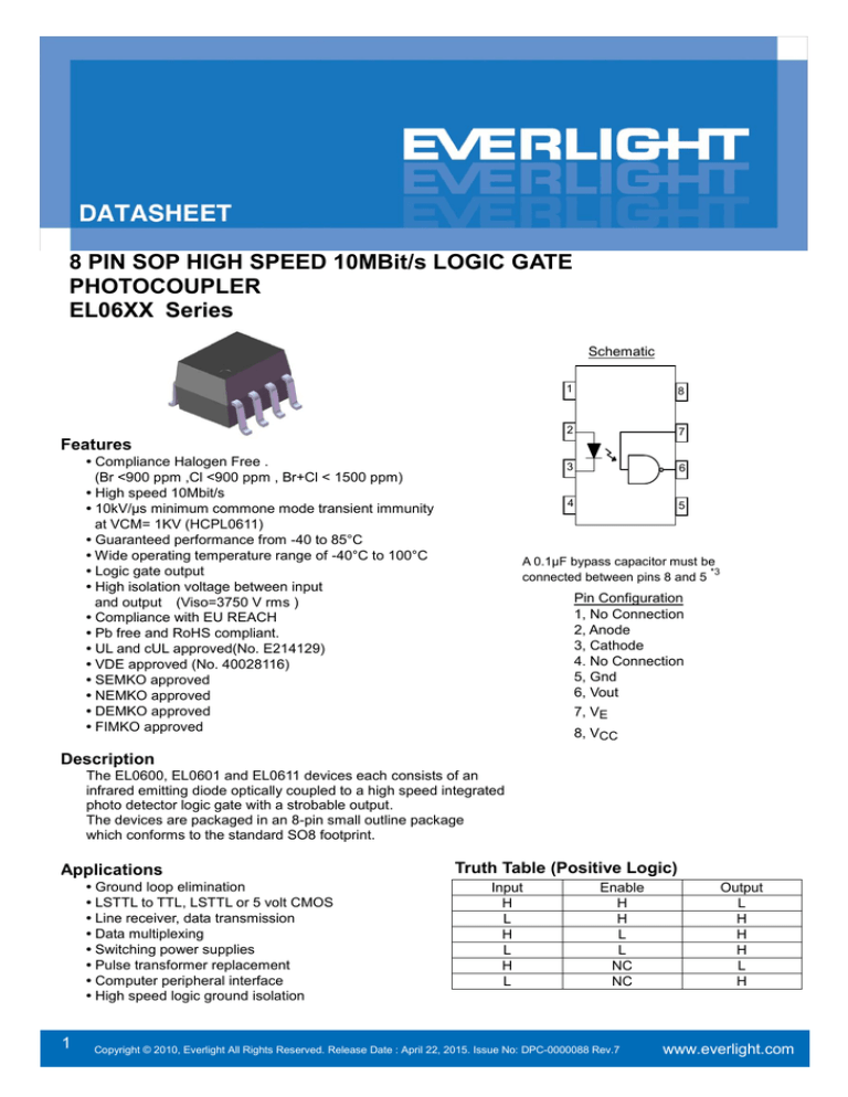
Schematic
1
8
2
7
3
6
4
5
Features
• Compliance Halogen Free .
(Br <900 ppm ,Cl <900 ppm , Br+Cl < 1500 ppm)
• High speed 10Mbit/s
• 10kV/μs minimum commone mode transient immunity
at VCM= 1KV (HCPL0611)
• Guaranteed performance from -40 to 85°C
• Wide operating temperature range of -40°C to 100°C
• Logic gate output
• High isolation voltage between input
and output (Viso=3750 V rms )
• Compliance with EU REACH
• Pb free and RoHS compliant.
• UL and cUL approved(No. E214129)
• VDE approved (No. 40028116)
• SEMKO approved
• NEMKO approved
• DEMKO approved
• FIMKO approved
A 0.1μF bypass capacitor must be
*3
connected between pins 8 and 5
Pin Configuration
1, No Connection
2, Anode
3, Cathode
4. No Connection
5, Gnd
6, Vout
7, VE
8, VCC
Description
The EL0600, EL0601 and EL0611 devices each consists of an
infrared emitting diode optically coupled to a high speed integrated
photo detector logic gate with a strobable output.
The devices are packaged in an 8-pin small outline package
which conforms to the standard SO8 footprint.
Applications
• Ground loop elimination
• LSTTL to TTL, LSTTL or 5 volt CMOS
• Line receiver, data transmission
• Data multiplexing
• Switching power supplies
• Pulse transformer replacement
• Computer peripheral interface
• High speed logic ground isolation
1
Truth Table (Positive Logic)
Input
H
L
H
L
H
L
Enable
H
H
L
L
NC
NC
Copyright © 2010, Everlight All Rights Reserved. Release Date : April 22, 2015. Issue No: DPC-0000088 Rev.7
Output
L
H
H
H
L
H
www.everlight.com
DATASHEET
8 PIN SOP HIGH SPEED 10MBit/s LOGIC GATE
PHOTOCOUPLER
EL06XX Series
Absolute Maximum Ratings (Ta=25°C)
Parameter
Symbol
Rating
Unit
Forward current
IF
20
mA
Enable input voltage Not exceed VCC
by more than 500mV
VE
5.5
V
Reverse voltage
VR
5
V
Power dissipation
PD
40
mW
Power dissipation
PC
85
mW
Enable input current
IE
5
mA
Output current
IO
50
mA
Output voltage
VO
7.0
V
Output Power Dissipation
PO
100
mW
VISO
3750
V rms
Operating temperature
TOPR
-40 ~ +100
°C
Storage temperature
TSTG
-55 ~ +125
°C
TSOL
260
°C
Input
Output
Isolation voltage
*1
Soldering temperature
*2
Notes:
*1 AC for 1 minute, R.H.= 40 ~ 60% R.H. In this test, pins 1, 2, 3 & 4 are shorted together, and pins 5, 6, 7 & 8 are shorted together.
*2 For 10 seconds.
2
Copyright © 2010, Everlight All Rights Reserved. Release Date : April 22, 2015. Issue No:DPC-0000088 Rev.7
www.everlight.com
DATASHEET
8 PIN SOP HIGH SPEED 10MBit/s LOGIC GATE
PHOTOCOUPLER
EL06XX Series
Electrical Characteristics (Ta=-40 to 85°C unless specified otherwise)
Input
Symbol
Min.
Typ.
Max.
Unit
Forward voltage
VF
-
1.4
1.8
V
IF = 10mA
Reverse voltage
VR
5.0
-
-
V
IR = 10μA
VF/TA
-
-1.8
-
mV/°C
IF =10mA
CIN
-
60
-
pF
VF=0, f=1MHz
Symbol
Min
Typ.
Max.
Unit
Condition
ICCH
-
-
10
mA
IF=10mA, VE=0.5V, VCC=5.5V
ICCL
-
-
13
mA
IF=0mA, VE=0.5V, VCC=5.5V
IEH
-
-
-1.6
mA
VE=2.0V, VCC=5.5V
IEL
-
-
-1.6
mA
VE=0.5V, VCC=5.5V
VEH
2.0
-
-
V
IF=10mA, VCC=5.5V
VEL
-
-
0.8
V
IF=10mA, VCC=5.5V
Parameter
Temperature
coefficient of forward
voltage
Input capacitance
Condition
Output
Parameter
High level supply
current
Low level supply
current
High level enable
current
Low level enable
current
High level enable
voltage
Low level enable
*4
voltage
Transfer Characteristics (Ta=-40 to 85°C unless specified otherwise)
Parameter
HIGH Level Output
Current
LOW Level Output
Current
Input Threshold
Current
3
Symbol
Min
Typ.
Max.
Unit
IOH
-
-
100
uA
VOL
-
-
0.6
V
IFT
-
-
5
mA
Condition
VCC=5.5V, VO=5.5V,
IF=250μA, VE=2.0V
VCC = 5.5V, IF=5mA,
VE=2.0V,ICL=13mA
VCC= 5.5V, VO=0.6V,
VE =2.0V,IOL=13mA
Copyright © 2010, Everlight All Rights Reserved. Release Date : April 22, 2015. Issue No:DPC-0000088 Rev.7
www.everlight.com
DATASHEET
8 PIN SOP HIGH SPEED 10MBit/s LOGIC GATE
PHOTOCOUPLER
EL06XX Series
Switching Characteristics (Ta=-40 to 85°C, VCC=5V, IF=7.5mA unless specified otherwise)
Parameter
Propagation delay
time to output High
5
level* (Fig.12)
Propagation delay
time to output Low
6
level* (Fig.12)
Pulse width distortion
Symbol
Min
Typ.
Max.
Unit
TPHL
-
35
75
ns
CL = 15pF, RL=350Ω,
TA=25°C
TPLH
-
45
75
ns
CL = 15pF, RL=350Ω,
TA=25°C
|Tphl – Tplh|
-
10
35
ns
CL = 15pF, RL=350Ω
tr
-
30
40
ns
CL = 15pF, RL=350Ω
tf
-
10
20
ns
CL = 15pF, RL=350Ω
Condition
7
Output rise time*
(Fig.12)
8
Output fall time*
(Fig.12)
Switching Characteristics (Ta=-40 to 85°C, VCC=5V, IF=7.5mA unless specified otherwise)
Symbol
Min
Typ.
Max.
Unit
Condition
tELH
-
30
40
ns
IF = 7.5mA , VEH=3.5V,
CL = 15pF, RL=350Ω
tEHL
-
20
30
ns
IF = 7.5mA , VEH=3.5V,
CL = 15pF, RL=350Ω
EL0600
-
-
-
EL0601
5,000
-
-
Parameter
Enable Propagation
Delay Time to Output
9
High Level*
(Fig.13)
Enable Propagation
Delay Time to Output
10
Low Level*
(Fig.13)
Common
Mode
Transient
Immunity
at Logic
*11
High
Common
Mode
Transient
Immunity
at Logic
*12
Low
4
V/µS
CMH
EL0611
10,000
-
-
EL0611
15,000
-
-
EL0600
-
-
-
EL0601
5,000
V/µS
CML
EL0611
10,000
-
-
EL0611
15,000
-
-
IF = 7.5mA , VOH=2.0V,
RL=350Ω, TA=25°C
VCM=10Vp-p (Fig.14)
IF = 7.5mA , VOH=2.0V,
RL=350Ω, TA=25°C
VCM=50Vp-p (Fig.14)
IF = 7.5mA , VOH=2.0V,
RL=350Ω, TA=25°C
VCM=400Vp-p (Fig.14)
IF = 7.5mA , VOH=2.0V,
RL=350Ω, TA=25°C
VCM=400Vp-p (Fig.15)
IF = 0mA , VOL=0.8V,
RL=350Ω, TA=25°C
VCM=10Vp-p (Fig.14)
IF = 0mA , VOL=0.8V,
RL=350Ω, TA=25°C
VCM=50Vp-p (Fig.14)
IF = 0mA , VOL=0.8V,
RL=350Ω, TA=25°C
VCM=400Vp-p (Fig.14)
IF = 7.5mA , VOL=0.8V,
RL=350Ω, TA=25°C
VCM=400Vp-p (Fig.15)
Copyright © 2010, Everlight All Rights Reserved. Release Date : April 22, 2015. Issue No:DPC-0000088 Rev.7
www.everlight.com
DATASHEET
8 PIN SOP HIGH SPEED 10MBit/s LOGIC GATE
PHOTOCOUPLER
EL06XX Series
Typical Electro-Optical Characteristics Curves
5
Copyright © 2010, Everlight All Rights Reserved. Release Date : April 22, 2015. Issue No:DPC-0000088 Rev.7
www.everlight.com
DATASHEET
8 PIN SOP HIGH SPEED 10MBit/s LOGIC GATE
PHOTOCOUPLER
EL06XX Series
6
Copyright © 2010, Everlight All Rights Reserved. Release Date : April 22, 2015. Issue No:DPC-0000088 Rev.7
www.everlight.com
DATASHEET
8 PIN SOP HIGH SPEED 10MBit/s LOGIC GATE
PHOTOCOUPLER
EL06XX Series
Fig. 12 Test circuit and waveforms for tPHL, tPLH, tr, and tf
Ω
IF=7.5mA
IF=3.75mA
Input
(IF)
tPHL
tPLH
Output
(Vo)
1.5V
90%
Ω
Output
(Vo)
10%
tf
tr
Fig. 13 Test circuit and waveform for tEHLand tELH
Ω
3.0V
Input
(VE)
1.5V
tEHL
tELH
Output
(Vo)
1.5V
7
Copyright © 2010, Everlight All Rights Reserved. Release Date : April 22, 2015. Issue No:DPC-0000088 Rev.7
www.everlight.com
DATASHEET
8 PIN SOP HIGH SPEED 10MBit/s LOGIC GATE
PHOTOCOUPLER
EL06XX Series
Fig. 14 Test circuit Common mode Transient Immunity
Ω
Peak
VCM
0V
5V
Vo
CMH
Switching Pos. (A), IF=0
VO(Min)
VO(Max)
Switching Pos. (B), IF=7.5mA
VCM
CML
0.5V
Fig. 15 Recommended drive circuit for EL0611 families for high-CMR
μ
Ω
8
Copyright © 2010, Everlight All Rights Reserved. Release Date : April 22, 2015. Issue No:DPC-0000088 Rev.7
www.everlight.com
DATASHEET
8 PIN SOP HIGH SPEED 10MBit/s LOGIC GATE
PHOTOCOUPLER
EL06XX Series
Notes
*3. The VCC supply must be bypassed by a 0.1μF capacitor or larger. This can be either a ceramic or solid tantalum
capacitor with good high frequency characteristic and should be connected as close as possible to the package
VCC and GND pins
*4. Enable Input – No pull up resistor required as the device has an internal pull up resistor.
*5. tPLH– Propagation delay is measured from the 3.75mA level on the HIGH to LOW transition of the input current
pulse to the 1.5 V level on the LOW to HIGH transition of the output voltage pulse.
*6. tPHL– Propagation delay is measured from the 3.75mA level on the LOW to HIGH transition of the input current
pulse to the 1.5 V level on the HIGH to LOW transition of the output voltage pulse.
*7. tr– Rise time is measured from the 90% to the 10% levels on the LOW to HIGH transition of the output pulse.
*8. tf– Fall time is measured from the 10% to the 90% levels on the HIGH to LOW transition of the output pulse.
*9. tELH– Enable input propagation delay is measured from the 1.5V level on the HIGH to LOW transition of the
input voltage pulse to the 1.5V level on the LOW to HIGH transition of the output voltage pulse.
*10. tEHL– Enable input propagation delay is measured from the 1.5V level on the LOW to HIGH transition of the
input voltage pulse to the 1.5V level on the HIGH to LOW transition of the output voltage pulse.
*11 CMH– The maximum tolerable rate of rise of the common mode voltage to ensure the output will remain in the
HIGH state (i.e., VOUT > 2.0V).
*12 CML– The maximum tolerable rate of rise of the common mode voltage to ensure the output will remain in the
LOW output state (i.e., VOUT < 0.8V).
Order Information
Part Number
EL06XX(Z)-V
Note
X = Part no. ( X = 00, 01 or 11)
Z = Tape and reel option (TA, TB or none).
V = VDE (optional)
Option
9
Description
Packing quantity
None
Standard
100 units per tube
-V
Standard + VDE
100 units per tube
(TA)
TA tape & reel option
2000 units per reel
(TB)
TB tape & reel option
2000 units per reel
(TA)-V
TA tape & reel option + VDE
2000 units per reel
(TB)-V
TB tape & reel option + VDE
2000 units per reel
Copyright © 2010, Everlight All Rights Reserved. Release Date : April 22, 2015. Issue No:DPC-0000088 Rev.7
www.everlight.com
DATASHEET
8 PIN SOP HIGH SPEED 10MBit/s LOGIC GATE
PHOTOCOUPLER
EL06XX Series
Package Dimension
(Dimensions in mm)
Recommended pad layout for surface mount leadform
10
Copyright © 2010, Everlight All Rights Reserved. Release Date : April 22, 2015. Issue No:DPC-0000088 Rev.7
www.everlight.com
DATASHEET
8 PIN SOP HIGH SPEED 10MBit/s LOGIC GATE
PHOTOCOUPLER
EL06XX Series
Device Marking
EL
0600
YWWV
Notes
EL
0600
Y
WW
V
11
denotes EVERLIGHT
denotes Device Number
denotes 1 digit Year code
denotes 2 digit Week code
denotes VDE (optional)
Copyright © 2010, Everlight All Rights Reserved. Release Date : April 22, 2015. Issue No:DPC-0000088 Rev.7
www.everlight.com
DATASHEET
8 PIN SOP HIGH SPEED 10MBit/s LOGIC GATE
PHOTOCOUPLER
EL06XX Series
Tape & Reel Packing Specifications
Option TB
Option TA
Direction of feed from reel
Direction of feed from reel
Tape dimension
12
Dimension No.
A0
A1
B0
D0
D1
E
F
Dimension(mm)
6.2±0.1
4.1±0.1
5.28±0.1
1.5±0.1
1.5±0.3
1.75±0.1
5.5±0.1
Dimension No.
Po
P1
P2
t
W
K0
K1
Dimension(mm)
4.0±0.1
8.0±0.1
2.0±0.1
0.4±0.1
3.7±0.1
0.3±0.1
12.0+0.3/
-0.1
Copyright © 2010, Everlight All Rights Reserved. Release Date : April 22, 2015. Issue No:DPC-0000088 Rev.7
www.everlight.com
DATASHEET
8 PIN SOP HIGH SPEED 10MBit/s LOGIC GATE
PHOTOCOUPLER
EL06XX Series
Precautions for Use
1. Soldering Condition
1.1 (A) Maximum Body Case Temperature Profile for evaluation of Reflow Profile
Note:
Reference: IPC/JEDEC J-STD-020D
Preheat
Temperature min (Tsmin)
150 °C
Temperature max (Tsmax)
200°C
Time (Tsmin to Tsmax) (ts)
Average ramp-up rate (Tsmax to Tp)
60-120 seconds
3 °C/second max
Other
Liquidus Temperature (TL)
217 °C
Time above Liquidus Temperature (t L)
60-100 sec
Peak Temperature (TP)
260°C
Time within 5 °C of Actual Peak Temperature: T P - 5°C
30 s
Ramp- Down Rate from Peak Temperature
6°C /second max.
Time 25°C to peak temperature
Reflow times
8 minutes max.
3 times
13
Copyright © 2010, Everlight All Rights Reserved. Release Date : April 22, 2015. Issue No:DPC-0000088 Rev.7
www.everlight.com
DATASHEET
8 PIN SOP HIGH SPEED 10MBit/s LOGIC GATE
PHOTOCOUPLER
EL06XX Series
DISCLAIMER
1. Above specification may be changed without notice. EVERLIGHT will reserve authority on material change for above
specification.
2. When using this product, please observe the absolute maximum ratings and the instructions for using outlined in these
specification sheets. EVERLIGHT assumes no responsibility for any damage resulting from use of the product which
does not comply with the absolute maximum ratings and the instructions included in these specification sheets.
3. These specification sheets include materials protected under copyright of EVERLIGHT corporation. Please don’t
reproduce or cause anyone to reproduce them without EVERLIGHT’s consent.
14
Copyright © 2010, Everlight All Rights Reserved. Release Date : April 22, 2015. Issue No:DPC-0000088 Rev.7
www.everlight.com


