Improved Transient Response Capacitor-less Low Drop
advertisement

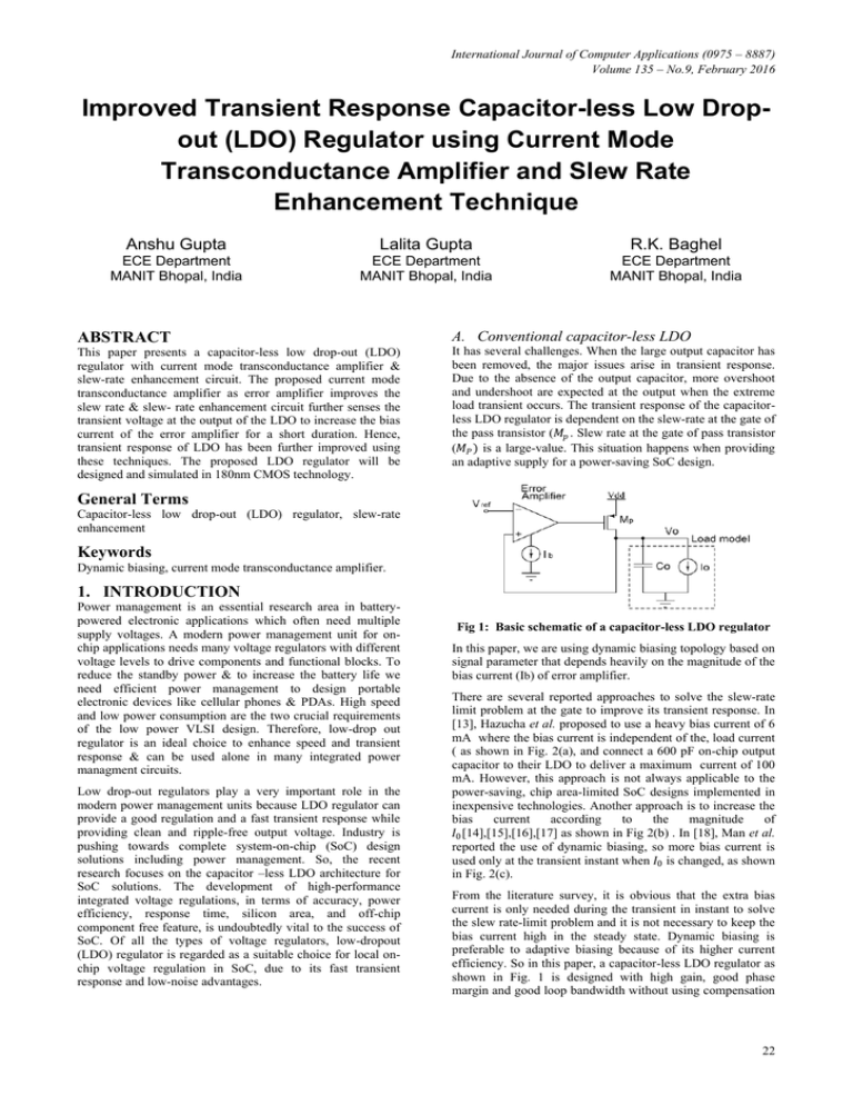
International Journal of Computer Applications (0975 – 8887) Volume 135 – No.9, February 2016 Improved Transient Response Capacitor-less Low Dropout (LDO) Regulator using Current Mode Transconductance Amplifier and Slew Rate Enhancement Technique Anshu Gupta Lalita Gupta R.K. Baghel ECE Department MANIT Bhopal, India ECE Department MANIT Bhopal, India ECE Department MANIT Bhopal, India ABSTRACT A. Conventional capacitor-less LDO This paper presents a capacitor-less low drop-out (LDO) regulator with current mode transconductance amplifier & slew-rate enhancement circuit. The proposed current mode transconductance amplifier as error amplifier improves the slew rate & slew- rate enhancement circuit further senses the transient voltage at the output of the LDO to increase the bias current of the error amplifier for a short duration. Hence, transient response of LDO has been further improved using these techniques. The proposed LDO regulator will be designed and simulated in 180nm CMOS technology. It has several challenges. When the large output capacitor has been removed, the major issues arise in transient response. Due to the absence of the output capacitor, more overshoot and undershoot are expected at the output when the extreme load transient occurs. The transient response of the capacitorless LDO regulator is dependent on the slew-rate at the gate of the pass transistor (𝑀𝑝 . Slew rate at the gate of pass transistor (𝑀𝑃 ) is a large-value. This situation happens when providing an adaptive supply for a power-saving SoC design. General Terms Capacitor-less low drop-out (LDO) regulator, slew-rate enhancement Keywords Dynamic biasing, current mode transconductance amplifier. 1. INTRODUCTION Power management is an essential research area in batterypowered electronic applications which often need multiple supply voltages. A modern power management unit for onchip applications needs many voltage regulators with different voltage levels to drive components and functional blocks. To reduce the standby power & to increase the battery life we need efficient power management to design portable electronic devices like cellular phones & PDAs. High speed and low power consumption are the two crucial requirements of the low power VLSI design. Therefore, low-drop out regulator is an ideal choice to enhance speed and transient response & can be used alone in many integrated power managment circuits. Low drop-out regulators play a very important role in the modern power management units because LDO regulator can provide a good regulation and a fast transient response while providing clean and ripple-free output voltage. Industry is pushing towards complete system-on-chip (SoC) design solutions including power management. So, the recent research focuses on the capacitor –less LDO architecture for SoC solutions. The development of high-performance integrated voltage regulations, in terms of accuracy, power efficiency, response time, silicon area, and off-chip component free feature, is undoubtedly vital to the success of SoC. Of all the types of voltage regulators, low-dropout (LDO) regulator is regarded as a suitable choice for local onchip voltage regulation in SoC, due to its fast transient response and low-noise advantages. Fig 1: Basic schematic of a capacitor-less LDO regulator In this paper, we are using dynamic biasing topology based on signal parameter that depends heavily on the magnitude of the bias current (Ib) of error amplifier. There are several reported approaches to solve the slew-rate limit problem at the gate to improve its transient response. In [13], Hazucha et al. proposed to use a heavy bias current of 6 mA where the bias current is independent of the, load current ( as shown in Fig. 2(a), and connect a 600 pF on-chip output capacitor to their LDO to deliver a maximum current of 100 mA. However, this approach is not always applicable to the power-saving, chip area-limited SoC designs implemented in inexpensive technologies. Another approach is to increase the bias current according to the magnitude of 𝐼0 [14],[15],[16],[17] as shown in Fig 2(b) . In [18], Man et al. reported the use of dynamic biasing, so more bias current is used only at the transient instant when 𝐼0 is changed, as shown in Fig. 2(c). From the literature survey, it is obvious that the extra bias current is only needed during the transient in instant to solve the slew rate-limit problem and it is not necessary to keep the bias current high in the steady state. Dynamic biasing is preferable to adaptive biasing because of its higher current efficiency. So in this paper, a capacitor-less LDO regulator as shown in Fig. 1 is designed with high gain, good phase margin and good loop bandwidth without using compensation 22 International Journal of Computer Applications (0975 – 8887) Volume 135 – No.9, February 2016 circuits and compensation capacitance. The dynamic biasing technique is implemented by a simple and effective slew rate enhancement circuit. The slew rate enhancement circuit makes use of the rapid transient voltage at the LDO output to increase the bias current of error amplifier for a short duration. Hence, the transient response of the LDO can be significantly improved due to the enhancement of slew rate at the gate of the pass transistor. conventional LDO regulator when 𝐼0 suddenly increases and decreases , respectively. When 𝐼0 rapidly increases, the LDO cannot change 𝑉𝑆𝐺 of pass transistor instantaneously to provide current due to the large parasitic capacitance (Cpar) at the gate of the pass transistor, and this situation causes output voltage (𝑉0 ) of LDO to drop. The drop of 𝑉0 reduces the 𝑉𝐺𝑆 of M1, and it causes M1 to cutoff momentarily. So the transistors M3 and M4 are also cut off momentarily. Thus 𝐼𝑏 is the discharging current of Cpar. Similarly, when 𝐼0 suddenly decreases, the LDO cannot reduce 𝑉𝑆𝐺 of pass transistor immediately and it makes 𝑉0 rise. The rise of 𝑉0 increases the 𝑉𝐺𝑆 of M1 and it causes M2 to cutoff momentarily. Therefore, the charging current of Cpar is 𝐼𝑏 . The pass transistor has a very large transconductance, but the large effective input gate capacitance limits its transient speed. The effective input gate capacitance is driven by the error amplifier. In order for the error amplifier to drive large capacitive loads, 𝐼𝑏 must be increased. The slew rate (SR) at the gate of pass transistor is given by (1). The bias current of error amplifier only affects the slew rate in (1), and then Cpar is the total effective input gate capacitance of the pass transistor. The fundamental problem still exists; the power must be increased to drive larger pass transistors. This forms the inherent trade-off between the power efficiency and the transient response. SR= 𝐼𝑏 𝐶𝑝𝑎𝑟 (1) It is clear from the above analysis that 𝐼𝑏 determines the slew rate at the gate of pass transistor. Higher bias current does enhance the transient response of the LDO regulator, but this approach consumes unnecessary power since then is no charge/discharge mechanism of Cpar in the steady state. Finally, the pass transistor size is very critical, since it determines the value of Cpar or, from another point of view, the required amount of the bias current to solve the slew rate limit problem So, a slew rate enhancement circuit will be proposed to increases the bias current of the error amplifier momentarily during transients only and it maintains bias current constant during steady state. Fig 2: (a) Constant biasing (b) Adaptive biasing (c) dynamic biasing In this paper, a CMOS capacitor-free LDO regulator, which employing a simple bias circuit, a slew rate enhancement circuit & current mode transconductance amplifier is designed. The slew rate enhancement circuit is designed to increase the slew rate of LDO regulator output voltage when the load current is suddenly switched from low to high. And the reported LDO regulator can achieve well characteristic in this paper. In Section II, the circuit analysis and design of the LDO regulator is described. Section III will show the proposed current mode transconductance amplifier. In Section IV, the proposed slew rate enhancement circuit is explained. Section V will show the LDO regulator with CTA & SRE techniques. Section VI will show the simulation results. Finally, the conclusions are given in Section VII. 2. TRANSIENT BEHAVIOR OF CONVENTIONAL LDO TOPOLOGY In Fig 1 the error amplifier is replaced by differential amplifier for whole schematic of conventional LDO topology. The conventional LDO regulator undergoes large signal transient response when there is rapid and large change of𝐼0 . Fig 3 and Fig 4 show the large signal responses of the Fig 3: Large signal response during undershoot 23 International Journal of Computer Applications (0975 – 8887) Volume 135 – No.9, February 2016 3. PROPOSED CURRENT MODE TRANSCONDUCTANCE AMPLIFIER Fig. 6 shows the proposed current mode transconductance amplifier (CTA) in which LCMFB technique isused to enhance the slew rate of the amplifier. When no differential voltage is applied to the input ports, I1 and I4 are equal to IB1 = IB2= IB. In this situation, no current flows through resistors R1 and R2. Fig 4: Large signal response during overshoot Fig 6: Proposed current mode transconductance amplifier 4. PROPOSED SLEW RATE ENHANCEMENT TECHNIQUE Fig 5: Conventional LDO regulator The modified proposed slew rate enhancement circuit is shown in Fig 7. The main idea of the slew rate enhancement circuit is to momentarily increase the bias current of the error amplifier of the LDO when voltage spikes appears at the LDO output in order to overcome the problem of the slew rate limit due to the large Cpar at the gate of the pass transistor. The slew rate enhancement circuit is effectively designed to produce fast response. In the slew rate enhancement circuit, transistors M17 and M18 will form a latch. The loop gain of the latch is taken as 0.9. There are two positive feedback loops created by M19-M21-M23 and M20-M22-M24 with loop gains less than unity. 24 International Journal of Computer Applications (0975 – 8887) Volume 135 – No.9, February 2016 Fig 7: Proposed slew rate enhancement circuit 5. PROPOSED CAPACITOR-LESS LDO REGULATOR The large signal operation of the proposed LDO regulator is as shown in Fig 8. During steady state operation, the 𝑉0 of LDO is 1.2V and the slew rate enhancement circuit produces a bias current (I3+I4) of the CTA which is 25µA. whenever large undershoot occurs in 𝑉0 of the LDO, then the 𝑉𝐺𝑆 of the transistor M10 goes low and it makes M10 to go into the cut off- region. Hence the drain voltage of M10 is increased. So the transistors M14, M16, M17, M18, and M20 are cut-off. The current in the transistor M13 is increased and due to positive feedback path through M19-M21-M23, the current in M13 will be further increased. Hence, the bias current of the CTA amplifier is increased to improve the transient response of LDO regulator. Whenever large overshoot occurs in 𝑉0 of the LDO, then the 𝑉𝐺𝑆 of the transistor M10 goes high. Hence the drain voltage M10 is decreased and same of M9 is increased. So the transistors M13, M15, M17, M18, and M19 are cut-off. The current in the transistor m14 is increased and due to positive feedback path through M20-M22-M24, the current in M13 will be further increased. Hence the bias current of the current mode transconductance amplifier is increased to improve the transient response of LDO regulator. 25 International Journal of Computer Applications (0975 – 8887) Volume 135 – No.9, February 2016 Fig 8: Proposed Capacitor-Less LDO regulator 6. SIMULATION RESULTS Fig 9 shows Transient response of LDO without using proposed SRE & CTA at 1 mA and 100 mA of load current. Fig 10 shows Transient response of LDO with using proposed SRE. Fig 11 represents Frequency response of Proposed LDO. Fig 12 shows Transient response of LDO with proposed SRE & CTA Fig 9: Transient response of LDO without using proposed SRE & CTA 26 International Journal of Computer Applications (0975 – 8887) Volume 135 – No.9, February 2016 Fig 10: Transient response of LDO with using proposed SRE Fig 11: Frequency response of Proposed LDO 27 International Journal of Computer Applications (0975 – 8887) Volume 135 – No.9, February 2016 Fig 12: Transient response of LDO with proposed SRE & CTA 7. CONCLUSION The transient response of a capacitor-less LDO regulator is dependent on the slew rate at the gate of the pass transistor. A slew-rate enhancement circuit has been proposed to solve the slew-rate limit problem at the gate of the pass transistor. In this paper, a CMOS low quiescent current in LDO regulator is also introduced based on a high slew rate CTA. The load transient characteristic of the LDO is improved by using a LCMFB technique in the proposed CTA which results in an increase of the nonlinear transfer characteristic order thereby enhancing the slew rate at the gate of pass transistor. The proposed capacitor-less LDO regulator with 100 pF parasitic capacitance of load is stable throughout the load range without using any compensation capacitance. The post layout simulation results have proven that the transient response of capacitor-less LDO has been improved significantly by proposed slew-rate enhancement circuit at different slew-rates of load current. It regulates the output voltage at 1.2 V from 1.4 V - 1.8 V supply, with a minimum drop-out voltage of 200 mV at the maximum output current of 100 mA without any internal compensation capacitor and with output capacitor in the range of 10–100pF. With the proposed LDO regulator, the amount of output voltage overshoot/undershoot at the extreme load transients and the settling time of the regulator are improved. 8. REFERENCES [1] G.A. Rincon-Mora, P.E. Allen.Optimized frequencyshaping circuit topologies for LDO’s. IEEE Trans Circuits Syst II, Analog Digit. Signal Process. vol.45, no.6, pp.703-708, Jun.1998. [2] K.N. Leung, P.K.T. Mok.A capacitor-free CMOS lowdropout regulator with damping-factor-control frequency compensation. IEEE J Solid- State Circuits, vol.38, no.10, pp.1691-1702, Oct. 2003. [3] R.J.Milliken, J.Silva-Mart´nez, E. S´anchezSinencio.Full on-chip CMOS low-dropout voltage regulator. IEEE Trans Circuits Syst I, Reg. Papers, vol.54, no.9, pp.1879-1890, Sept. 2007. [4] W.H.Hung, S.H.Lung, and S.I.Liu. A capacitorfreeCMOS low dropout regulator with slew rate enhancement. In Int. symposium on VLSI Design, Automation and Test, 2006, pp.1-4 [5] C.M.Chen,and C.C.Hung.A capacitor-free CMOS lowdropout voltage regulator. In IEEE Int.symposium on circuits and systems,2009, pp.2525-2528. [6] X. Liu, S. Guo, and Y.C. Chang. Design of off-chip capacitor-free CMOS low-dropout voltage regulator. In IEEE Asia Pacific conference on circuits and systems, 2008, pp.1316-1319. [7] E.N.Y. Ho, and P.K.T. Mok. A capacitor-less CMOS active feedback low-dropout regulator with slew-rate enhancement for portable on-chip application. IEEE Trans Circuits Syst II:express briefs. Vol.57, no.2, pp.80-84, Feb. 2010. [8] T.Y. Man, K.N. Leung, C.Y. Leung, P.K.T. Mok, and M. Chan. Development of single-transistor- control LDO based on flipped voltage for SoC. IEEE Trans Circuits Syst I, Reg. Papers, vol.55, no.5, pp.1392-1401, Jun. 2008. [9] P.Y. Or, and K.N. Leung. An output-capacitorless lowdropout regulator with direct voltage-spike detection. IEEE J Solid-State Circuits, vol.45, no.2, pp.458-466, Feb. 2010. [10] K. N. Leung and P. K. T. Mok, “A capacitor-free CMOS low-dropout regulator with damping-factor-control 28 International Journal of Computer Applications (0975 – 8887) Volume 135 – No.9, February 2016 frequency compensation,” IEEE J. Solid-State Circuits, vol.38, no. 10, pp. 1691–1702, Oct. 2003. [11] S. K. Lau, P. K. T. Mok, and K. N. Leung, “A lowdropout regulator for SoC with Q-reduction,” IEEE J. Solid-State Circuits, vol. 42, no. 3, pp. 658–664, Mar. 2007. [12] Milliken, R.J.; Silva-Martinez, J.; Sanchez Sinencio, E.; "Full On-Chip CMOS Low-Dropout Voltage Regulator," Circuits and Systems I: Regular Papers, IEEE Transactions on , vol.54, no.9, pp.1879-1890, Sept. 2007. [13] P. Hazucha, T. Karnik, B. A. Bradley, C. Parsons, D. Finan, and S. Borkar, “Area-efficient linear regulator with ultra-fast load regulation,” IEEE J. Solid-State Circuits, vol. 40, no. 4, pp. 933–940, Apr. 2005. [14] Y.-H. Lam and W.-H. Ki, “A 0.9 V 0.35 μm adaptively biased CMOS LDO regulator with fast transient response,” in IEEE Int. Solid-State Circuits Conf. Dig. Tech. Papers, Feb. 2008, pp. 442–443, 626. [15] Ali Enayat Zadeh and Yung-I Chang, “Linear voltage regulator using adaptive biasing”, United States Patent IJCATM : www.ijcaonline.org US 6,522,111 B2, February 18, 2003 (United States Patent Application no. US 2002/0130646 A1 September 19, 2002). [16] Jaideep Banerjee and Tushar S Nandurkar, “Voltage regulator with improved load regulation using adaptive biasing”, United States Patent US 6,933,772 B1, August 23, 2005. [17] Matthias Eberlein, “Adaptive biasing concept for current mode voltage regulators”, United States Patent US 7,166,991 B2, January 23, 2007. [18] T. Y. Man, P. K. T. Mok, and M. Chan, “A high slewrate push-pull output amplifier for low- quiescent current low-dropout regulators with transient-response improvement,” IEEE Trans.Circuits Syst. II, Exp. Briefs, vol. 54, no. 9, pp. 755–759, Sep. 2007. [19] P. Y. Or and K. N. Leung, “An output capacitorless lowdropout regulatorwith direct voltage-spike detection,” IEEE J. Solid-State Circuits, vol. 45,no. 2, pp. 458–466, Feb. 2010. 29


