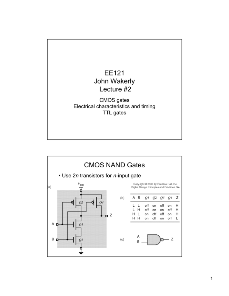
EE121 John Wakerly Lecture #2 CMOS NAND Gates
advertisement

EE121 John Wakerly Lecture #2 CMOS gates Electrical characteristics and timing TTL gates CMOS NAND Gates • Use 2n transistors for n-input gate 1 • CMOS NAND -- switch model • CMOS NAND -- more inputs (3) 2 • Inherent inversion. • Non-inverting buffer: • 2-input AND gate: 3 CMOS NOR Gates • Like NAND -- 2n transistors for n-input gate NAND vs. NOR • For a given silicon area, PMOS transistors are “weaker” than NMOS transistors. NAND NOR • Result: NAND gates are preferred in CMOS. 4 Limited # of inputs in one gate • 8-input CMOS NAND Fancy stuff • CMOS AND-ORINVERT gate 5 CMOS Electrical Characteristics • Digital analysis works only if circuits are operated in spec: – Power supply voltage – Temperature – Input-signal quality – Output loading • Must do some “analog” analysis to prove that circuits are operated in spec. – Fanout specs – Timing analysis (setup and hold times) DC Loading • An output must sink current from a load when the output is in the LOW state. • An output must source current to a load when the output is in the HIGH state. 6 Output-voltage drops • Resistance of “off” transistor is > 1 Megohm, but resistance of “on” transistor is nonzero, – Voltage drops across “on” transistor, V = IR • For “CMOS” loads, current and voltage drop are negligible. • For TTL inputs, LEDs, terminations, or other resistive loads, current and voltage drop are significant and must be calculated. Example loading calculation • Need to know “on” and “off” resistances of output transistors, and know the characteristics of the load. 7 Calculate for LOW and HIGH state Limitation on DC load • If too much load, output voltage will go outside of valid logic-voltage range. • VOHmin, VIHmin • VOLmax, VILmax 8 Output-drive specs • VOLmax and VOHmin are specified for certain output-current values, IOLmax and IOHmax. – No need to know details about the output circuit, only the load. Input-loading specs • Each gate input requires a certain amount of current to drive it in the LOW state and in the HIGH state. – IIL and IIH – These amounts are specified by the manufacturer. • Fanout calculation – (LOW state) The sum of the IIL values of the driven inputs may not exceed IOLmax of the driving output. – (HIGH state) The sum of the IIH values of the driven inputs may not exceed IOHmax of the driving output. – Need to do Thevenin-equivalent calculation for nongate loads (LEDs, termination resistors, etc.) 9 Manufacturer’s data sheet TTL Electrical Characteristics 10 TTL LOW-State Behavior TTL HIGH-State Behavior 11 TTL Logic Levels and Noise Margins • Asymmetric, unlike CMOS • CMOS can be made compatible with TTL – “T” CMOS logic families CMOS vs. TTL Levels CMOS levels TTL levels CMOS with TTL Levels -- HCT, FCT, VHCT, etc. 12 TTL differences from CMOS • Asymmetric input and output characteristics. • Inputs source significant current in the LOW state, leakage current in the HIGH state. • Output can handle much more current in the LOW state (saturated transistor). • Output can source only limited current in the HIGH state (resistor plus partially-on transistor). • TTL has difficulty driving “pure” CMOS inputs because VOH = 2.4 V (except “T” CMOS). AC Loading • AC loading has become a critical design factor as industry has moved to pure CMOS systems. – CMOS inputs have very high impedance, DC loading is negligible. – CMOS inputs and related packaging and wiring have significant capacitance. – Time to charge and discharge capacitance is a major component of delay. 13 Transition times Circuit for transition-time analysis 14 HIGH-to-LOW transition Exponential rise time 15 LOW-to-HIGH transition Exponential fall time t = RC time constant exponential formulas, e-t/RC 16 Transition-time considerations • Higher capacitance ==> more delay • Higher on-resistance ==> more delay • Lower on-resistance requires bigger transistors • Slower transition times ==> more power dissipation (output stage partially shorted) • Faster transition times ==> worse transmission-line effects (Chapter 11) • Higher capacitance ==> more power dissipation (CV2f power), regardless of rise and fall time Open-drain outputs • No PMOS transistor, use resistor pull-up 17 What good is it? • Open-drain bus • Problem -- really bad rise time Open-drain transition times • Pull-up resistance is larger than a PMOS transistor’s “on” resistance. • Can reduce rise time by reducing pull-up resistor value – But not too much 18 Additional topics to read about • Wired Weird logic Logic • LEDs • Fighting outputs 19


