Volume 2, Issue 12, December-2015, pp. 1228-1231
ISSN (O): 2349-7084
International Journal of Computer Engineering In Research Trends
Available online at: www.ijcert.org
Investigation on Performance of high speed
CMOS Full adder Circuits
1
KATTUPALLI KALYANI, 2G.VASANTH RAO
1
2
(M.Tech) VLSI, Dept. of ECE
Assistant Professor, Dept. of ECE
Priyadarshini Institute of Technology & Science for Women
Abstract--- In this paper we demonstrate the performance analysis of CMOS Full adder circuits in this connection the
full Adder is designed using CMOS logic style by dividing it in three modules so that it can be optimized at various levels.
First module is an XOR-XNOR circuit, which generates full swing XOR and XNOR outputs simultaneously and have a
good driving capability. The objective this concept is identified the comparison of power, surface area and complexity of
Full adder designs using CMOS Logic Styles. Full adder Design is better compared to conventional design. Transistor
Design with respect to power, delay, Power Delay Product Comparison. It is observed that less power is consumed in the
Transmission based full adder than the Convention full adder and Pass Transistor full adder .
Keywords--- High speed, low power. CMOS logic style, full adder.
—————————— ——————————
1. INTRODUCTION
In very large scale integration (VLSI) systems, full
adder circuit is used in arithmetic operations for
addition, multipliers and Arithmetic Logic Unit
(ALU). It is a building block of the application of
VLSI, digital signal processing, image processing and
microprocessors. Most of full adder systems are
considered performance of circuits, number of
transistor, speed of circuit, chip area, threshold loss
and full swing output and the most important is
power consumption. In the future, portable devices
such as cell phone, laptop computer, tablet etc. that
need a low power and high speed for components are
requirements. For this reason, design of low power is
the research problems. In the paper is proposed I-bit
full adder base on 22 nm CMOS technology which
operation for low supply voltage is 1.2V at 250 MHz.
Full adder circuit is designed for addition binary
logics. Sum signal (SUM) and carry out signal (COUT)
are the output of I-bit full adder. Both of them are
generated by input A, B and CIN
© 2015, IJCERT All Rights Reserved
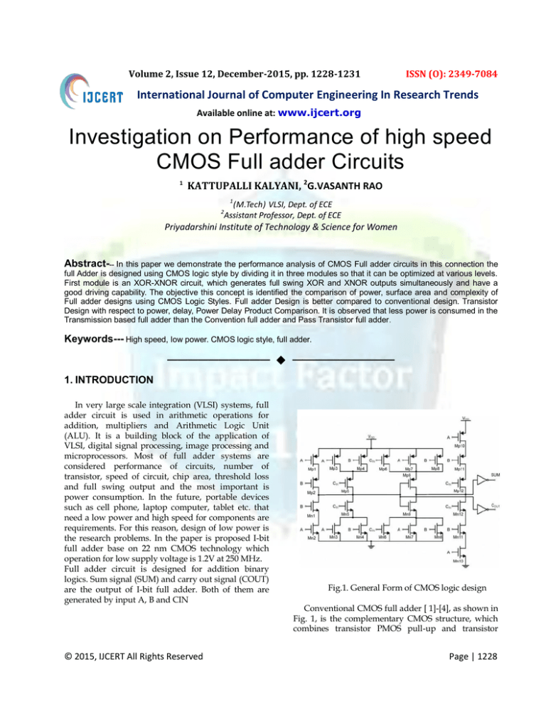
Fig.1. General Form of CMOS logic design
Conventional CMOS full adder [ 1]-[4], as shown in
Fig. 1, is the complementary CMOS structure, which
combines transistor PMOS pull-up and transistor
Page | 1228
Kalyani et al., International Journal of Computer Engineering In Research Trends
Volume 2, Issue 12, December-2015, pp. 1228-1231
NMOS pull-down network to produce output. The
complementary CMOS logic circuit has the advantage
of layout regularity and stability at low voltage. It has
a high transistor count which consumes area and
power. The problem of this adder is delay imbalance.
Because SUM signal relies on the generation of COUT
signal, there is a delay between two signals. The
transmission gate full adder is illustrated in Fig. 2,
which based on transmission gate [5]. It has lowertransistor count and lower loading of the input. After
generated, SUM and COUT signal are balanced than
the Conventional CMOS full adder. It provides
transistor buffer output of SUM and COUT for a high
driving capability. In Fig. 3 shows the hybrid logic full
adder [6]. It improves performance of speed and
driving capability. A weak point of this circuit is
separating between SUM and COUT circuits.
high switching speed
small area consumption
low power dissipation
CMOS Logic Inverter
2. CMOS LOGIC DESIGN
2.1 CMOS Technology:
Complementary
metal–oxide–semiconductor
(CMOS) is a technology for constructing integrated
circuits. CMOS is also sometimes referred to as
complementary-symmetry
metal–oxide
semiconductor (or COS-MOS). CMOS technology uses
both nMOS and pMOS transistors. The transistors are
arranged in a structure formed by two
complementary networks
Pull-up network is complement of pull-down
Parallel -> series, series -> parallel
Static and Dynamic CMOS Logic
Fig 3.a. Inverter Schematic symbol b.
2.2 CMOS Process Enhancements:
1) Silicon on Insulator:
As the name suggests transistors are fabricated on
an insulator (SiO2 or sapphire) Insulating substrate
eliminates capacitance between the source/drain and
body, higher speed devices and low leakage currents.
2) Transistors:
Multiple threshold voltages and oxide thicknesses
Processes offer multiple threshold voltages Low
threshold devices: faster, higher leakage.
2.3 Design and Architecture of Full Adder:
Meaning of Static and Dynamic CMOS Logic
Fig 2. Static and Dynamic CMOS Logic
Static design:
high functional reliability
easy circuit design
unlimited validity of logic outputs
Dynamic design:
© 2015, IJCERT All Rights Reserved
Page | 1229
Kalyani et al., International Journal of Computer Engineering In Research Trends
Volume 2, Issue 12, December-2015, pp. 1228-1231
Fig.4. 3-.4bit full adder
Table1. Truth table adder design
Fig.5. The gate level implementation for explanation
of full adder
The ultimate goal of a binary full-adder (BFA) is to
implement the following truth table for each bit:
Logically, carry = AB+BC+CA and Sum =
C⊕B⊕A, where k is an integer 0 to n for an n-bit
adder. Generally, adders of n-bits are created by
chaining together n of these 1-bit adder slices.
IMPORTANT TECHNICAL CONCEPTS
Transient (AC) Characteristic as well as Rise-Time,
Fall-Time and Delay Time
Rise-, Fall- and Delay-Time
Rise-Time tr Time for a transient waveform to rise
from 10% to 90% of its steady state values.
Fall-Time tf Time for a transient waveform to fall
from 90% to 10% of its steady state values.
Delay-Time td Time difference from the 50%
transition level of the input waveform to the 50%
transition level of the output waveform.
3. EXISTING SYSTEM DESIGN
Digital schematic is designed using DSCH for full
adder using 28 transistors which occupies a lot of
surface area and power consumed is also high which
can be reduced by reducing number of transistors.
The complexity can be decreased by modifying this
existing full adder design.The twenty eight bit
transistor based on regular CMOS structure i.e. pullup and pull-down network. One of the most
significant advantages of this full adder waists high
noise margins and thus reliable operation at low
voltages.
© 2015, IJCERT All Rights Reserved
Here implementation of the full adder circuit is
designed by taking the logic equations and
translate them directly into complementary CMOS
circuit in fig. . Some logic manipulations can help to
reduce the transistor count. For instance, it is
advantageous to share some logic between the sum
and carry – generation sub circuits, as long as this
does not slow down the carry generation, Which is
the most critical part as stated previously. The
following is an example of Such as reorganized
equation set:
Cout = A.B + B.Cin + A.Cin
S = A.B.Cin + Cout (A + B + Cin)
The equivalence with the original equations is
easily verified. The corresponding adder design,
using complementary static CMOS, is shown in
figure and the gate level implementation is shown
in figure. The transistors of the circuit produce the
Cout and the remaining transistors produce the Sum
outputs. Therefore the delay for computing Cout is
added to the total propagation delay of the Sum
output. The structure of this adder circuit is huge
and thereby consumes large on-chip area.
4. POWER DISSIPATION
There are three sources of power dissipation viz.
static power, dynamic power and short circuit
power dissipation. Static power dissipation is
associated with leakage current and can be
improved with the advancement in fabrication
technology only. Dynamic power dissipation is
given by the following equation:
Pd ═ αCL VDD2fCLK
Page | 1230
Kalyani et al., International Journal of Computer Engineering In Research Trends
Volume 2, Issue 12, December-2015, pp. 1228-1231
Where α is the switching activity, is the load
capacitance, VDD is the supply voltage and fCLK is
the clock frequency.
‹ Basic CMOS combinational circuits consist of: •
Complementary pull-up (p-type) and pull-down (ntype)
than most of the standard full-adder cells owing to
the novels design modules. Also it has been shown
that reducing the supply voltage is the most direct
means of reducing dissipated power and operating
CMOS devices is considered to be the most energyefficient solution for low-performance applications.
It performs well with supply voltage ranging from
1.2V to 2.4V. When embedded in a parallel adder
chain, it outperforms all the other adders making it
suitable for larger arithmetic circuits. Hence
reduced complexity is achieved by using less
number of transistors. Also power is reduced up to
30% in comparison to conventional design.
6. REFERENCES
[1] N. Weste, and K. Eshranghian, “Principles of
CMOS VLSI Design: A System Perspective,” Reading
MA: Wesley, 1993.
Fig 6. Static CMOS Circuit
Other source of power dissipation is short circuit
power dissipation that arises when direct current
flows from VDD to ground. Short circuit power
dissipation, depends on rise time and fall time
because it is only during transition that transistors
between VDD and ground remains on and short
circuit power dissipation comes into play. In the
optimized full adder circuit, both transistor count
and area has been reduced that lowers the dynamic
power dissipation as well as short circuit power
dissipation and hence the total power dissipation
reduces.
Table 2. Comparison among various Adders
Circuit (Full
Adder)
[2] Sanjeev Kumar and Manoj Kumar “4-2
Compressor design with New XOR-XNOR Module”,
4th International Conference on Advanced Computing
and Communication technologies, pp. 106-111, 2014.
[3] Meher, P.; Mahapatra, K.K. "Low power noise
tolerant domino 1-bit full adder", International
Conference on Advances in Energy Conversion
Technologies (ICAECT), pp. 125 – 129, 2014
[4] Vojin G. Oklobdzija, “Simple and Efficient Circuit
for Fast VLSI Adder Realization,” IEEE International
Symposium on Circuits and Systems Proceedings,
1988, pp. 1-4.
[5] J.Rabaey, “Digital Integrated Circuits: A Design
Prospective,” Prentice- Hall, Englewood Cliffs, NJ,
1996.
Power
180 nm
90 nm
45nm
CMOS Full Adder
3.998E-6
348.9E-9
79.12E-9
TG Full adder
1.519E-6
180.7E-9
24.86E-9
[6] R. Zimmermann and W. Fichtner, “Low-power
logic styles: CMOS versus pass-transistor logic,” IEEE
Journal of Solid–State Circuits, vol.32, pp.1079-1090,
July 1997.
[7] http://en.wikipedia.org/wiki/CMOS
Pass Transistor
Full Adder
1.823E-6
251.8E-9
27.36E-9
5. CONCLUSION
[8] Devi, Padma, Ashima Girdher, and Balwinder
Singh. "Improved carry select adder with reduced
area and low power consumption." International
Journal of Computer Applications 3.4 (2010): 14-18.
[9] D. Radhakrishnan, “Low-voltage low-power
CMOS full adder,” IEEE Proc. Circuits Devices Syst.,
vol. 148, no. 1, pp. 19–24, Feb. 2001.
The CMOS full adder has better performance
© 2015, IJCERT All Rights Reserved
Page | 1231
Kalyani et al., International Journal of Computer Engineering In Research Trends
Volume 2, Issue 12, December-2015, pp. 1228-1231
© 2015, IJCERT All Rights Reserved
Page | 1232


