a novel converter: matrix converters
advertisement

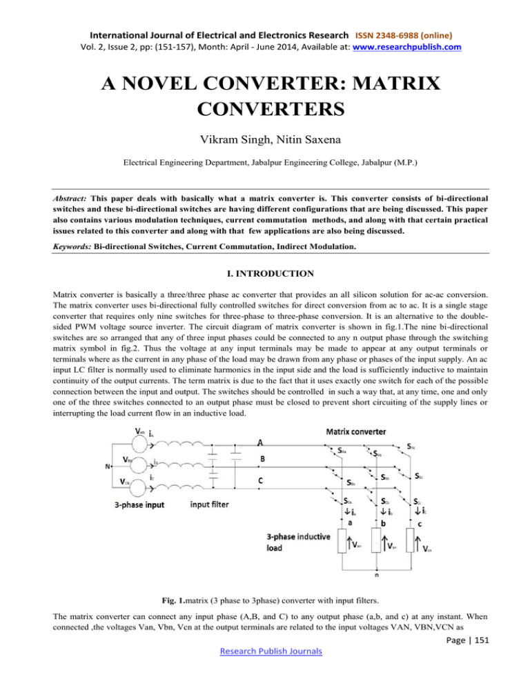
International Journal of Electrical and Electronics Research ISSN 2348-6988 (online) Vol. 2, Issue 2, pp: (151-157), Month: April - June 2014, Available at: www.researchpublish.com A NOVEL CONVERTER: MATRIX CONVERTERS Vikram Singh, Nitin Saxena Electrical Engineering Department, Jabalpur Engineering College, Jabalpur (M.P.) Abstract: This paper deals with basically what a matrix converter is. This converter consists of bi-directional switches and these bi-directional switches are having different configurations that are being discussed. This paper also contains various modulation techniques, current commutation methods, and along with that certain practical issues related to this converter and along with that few applications are also being discussed. Keywords: Bi-directional Switches, Current Commutation, Indirect Modulation. I. INTRODUCTION Matrix converter is basically a three/three phase ac converter that provides an all silicon solution for ac-ac conversion. The matrix converter uses bi-directional fully controlled switches for direct conversion from ac to ac. It is a single stage converter that requires only nine switches for three-phase to three-phase conversion. It is an alternative to the doublesided PWM voltage source inverter. The circuit diagram of matrix converter is shown in fig.1.The nine bi-directional switches are so arranged that any of three input phases could be connected to any n output phase through the switching matrix symbol in fig.2. Thus the voltage at any input terminals may be made to appear at any output terminals or terminals where as the current in any phase of the load may be drawn from any phase or phases of the input supply. An ac input LC filter is normally used to eliminate harmonics in the input side and the load is sufficiently inductive to maintain continuity of the output currents. The term matrix is due to the fact that it uses exactly one switch for each of the possible connection between the input and output. The switches should be controlled in such a way that, at any time, one and only one of the three switches connected to an output phase must be closed to prevent short circuiting of the supply lines or interrupting the load current flow in an inductive load. Fig. 1.matrix (3 phase to 3phase) converter with input filters. The matrix converter can connect any input phase (A,B, and C) to any output phase (a,b, and c) at any instant. When connected ,the voltages Van, Vbn, Vcn at the output terminals are related to the input voltages VAN, VBN,VCN as Page | 151 Research Publish Journals International Journal of Electrical and Electronics Research ISSN 2348-6988 (online) Vol. 2, Issue 2, pp: (151-157), Month: April - June 2014, Available at: www.researchpublish.com Fig. 2. Matrix switching. where as SAa through SCc are the switching variables of the corresponding switches. The switching function of a single switch as [2], (1) From above constraints it can be expressed as, =1, . (2) With these restrictions this converter has 27 possible switching states. Load and source voltages can expressed as vectors; = and = (3) = (4) = Where T is the instantaneous transition matrix. Similarly for input and output currents; = and = (5) = (6) = Where is the transpose matrix of T. In order to derive the rules for modulation it is compulsory to consider the switiching pattern that is employed,a similar for as given in [2]. Let be the duty cycle of switch , defined as , = , that can have following values: (7) Low fequency transfer matrix can be defined by; (8) Page | 152 Research Publish Journals International Journal of Electrical and Electronics Research ISSN 2348-6988 (online) Vol. 2, Issue 2, pp: (151-157), Month: April - June 2014, Available at: www.researchpublish.com Low frequency component of the output phase voltage is; (9) Low frequency component of the input current is; = . (10) (a) (b) Fig. 3. Waveforms (a) phase output voltage (b)load current. The matrix converter should be controlled using a specific and approximately time sequence of the values of the switching variables, which result in balanced output voltages having the desired frequency and amplitude, whereas the input currents are balanced and in phase with respect to the input voltages. However the the maximum peak to peak output voltage cannot be be greater than the minmum voltage difference between the two phases of the input. Regardless of the switching strategy, there is a physical limit on the achievable output voltage and the maximum voltage transfer ratio is 0.866. II. BI-DIRECTIONAL SWITCH 2.1 Realization with Discrete Semiconductors A first key problem is related to the bi-directional switches realization. By definition, a bidirectional switch is capable of conducting currents and blocking voltages of both polarities, depending on control actual signal. But at present time a true bi-directional switch is still not available on the market, and thus it must be realized by the combination of conventional unidirectional semiconductor devices. Fig.4 shows different bi-directional switch configurations which have been used in prototype and/or proposed in literature. Another problem, tightly related to the bi-directional switches implementation, which has represented a main obstacle to the industrial success of the matrix converter, is the commutation problem. The commutation issue basically rises from the absence, in the matrix converters, of static freewheeling paths. As consequence it becomes a difficult task to safely commutate the 20 current from one bi-directional switch to another, since a particular care is required in the timing and synchronisation of the switches command signals. Page | 153 Research Publish Journals International Journal of Electrical and Electronics Research ISSN 2348-6988 (online) Vol. 2, Issue 2, pp: (151-157), Month: April - June 2014, Available at: www.researchpublish.com Fig. 4. Possible discrete implementations of a bi-directional switch. (a) (b) (c) Diode Bridge with a single diode. Two anti-parallels IGBT with series diode. Two anti-parallel NPT-IGBT’s with reverse blocking capability. 2.2 Current Commutation Since there are no freewheel paths likewise in other conventional voltage source inverters the probability of attaining reliable current commutation is very less. For this there are two basic rules that to be considered; firstly no two bidirectional switches should be on at any one time. This will led to line to line short circuits and may damage the converter due to such large value of currents. Secondly , at any point in a time for each output phase the bi-directional switches should not at all be turned off. Current direction based commutation a four-step commutation strategy in which the direction of current flow through the commutation cells can be controlled. To implement this strategy the bi-directional switch must be designed in such a way as to allow the direction of the current flow in each switch to be controlled. Other commutation related problems relies on knowledge of the relative magnitudes of the input voltages instead of considering the direction of the output currents. Switches are then opened to block the reverse voltages. From this information a twostep or four-step commutation strategy can be formed in a similar way to the two-step and four-step current direction based commutation techniques. 2.3 Modulation Techniques (a) Basic Modulation Solution Normally modulation problem considered for this converter can be explained as, Given a set of input voltages and an assumed set of output currents = Find a modulation matrix such that and Page | 154 Research Publish Journals International Journal of Electrical and Electronics Research ISSN 2348-6988 (online) Vol. 2, Issue 2, pp: (151-157), Month: April - June 2014, Available at: www.researchpublish.com (12) And also the constraint equation (2) is satisfied. Here q is the voltage gain between the output and input voltages. There are two basic solutions [3],[4],[5] are shown; (13) With (14) With A direct transfer function is represented in this above given solution and is characterised by the fact that,during each time sequence time ( ) ,the average output voltage equals to the demand voltage. This could be possible when the target voltages must fit within the input voltage envelope for any output frequency, which leads to a limitation of the maximum voltage ratio. (B) Indirect Modulatin Methods These methods can increase the maximum voltage ratio above the 86.6% limit as compare to other methods [6], [7]. To do this modulation process defined in equation (9) is split into two steps as; )B (15) Where (16) Hence, = And B= (17) (18) Hence, (19) Where, q (voltage ratio) = (20) Here the A and B modulation are not continuous in time as shown above, but must be implemented by a suitable choice of the switching states. Page | 155 Research Publish Journals International Journal of Electrical and Electronics Research ISSN 2348-6988 (online) Vol. 2, Issue 2, pp: (151-157), Month: April - June 2014, Available at: www.researchpublish.com To maximize the voltage ratio, step A is implemented so that most positive and negative input voltages are selected continuously. No having maximum value of with a fictious dc link of . represents modulation index of a PWM process [6]. Now the overall voltage ratio has the maximum value of . 2.4 Some Practical Issues Over Voltage Protection: In a matrix converter, overvoltage can appear from the input side, originated by line perturbations. Also, dangerous overvoltage can appear from the output side, caused by an over current fault. When the switches are turned off, the current in the load is suddenly interrupted. The energy stored in the motor inductance has to be discharged without creating dangerous over voltages. A clamp configuration uses six diodes from the bidirectional switches to reduce the extra diodes to six [8]. A different overvoltage protection strategy replaces the clamp by varistors connected at the input and at the output terminals, plus a simple extra circuit to protect each IGBT [9]. In [10], controlled shutdown of the converter without using a clamp is proposed. This strategy uses controlled freewheeling states to reduce the motor current to zero, avoiding the generation of over voltages. Fig. 5. Matrix converter with clamp. Ride Through Capability: Ride-through capability is a desired characteristic in modern drives [11], [12]. A common solution is to decelerate the drive during power loss, receiving energy from the load inertia to feed the control electronics and to magnetize the motor. This is achieved by maintaining a constant voltage in the dc-link capacitor. Matrix converters do not have a dc-link capacitor and, for this reason, the previously mentioned strategy cannot be used. Fig. 6 shows a configuration proposed to provide short-termride-through capability to a matrix converter using the clamp capacitor as the source for a switch-mode power supply which feeds the converter control circuit [28]. After detection of a perturbation in the power supply, the motor is disconnected from the grid, but the switches of the matrix converter do not interrupt the motor currents. By applying the zero voltage vector (short circuit of the motor leads), the stator currents and the energy stored in the leakage inductance increases. The disconnection of the active switches originates the conduction of the clamp capacitor. This energy is then used to feed the control circuits. A flux and speed observer is used to restart the drive from nonzero flux and speed conditions in the shortest time. Fig. 6. Configuration to achieve ride-through capability Page | 156 Research Publish Journals International Journal of Electrical and Electronics Research ISSN 2348-6988 (online) Vol. 2, Issue 2, pp: (151-157), Month: April - June 2014, Available at: www.researchpublish.com III. CONCLUSION From the above given contents it is clear that what basically a matrix converter is, its various configurations of bidirectional switches, current commutation,and basic modulation techniques,. Matrix converters can be used as applications where power carries a premium such as integrated motor drives, aerospace, and marine propulsions. The matrix converter could be an ideal converter topology to utilise future technologies such as high temperature silicon carbide devices. These devices will operate at temperatures up to 300°C so the lack of large electrolytic capacitors, as normally used in an inverter, would again be a significant advantage. REFERENCES [1] Wheeler, P W., Rodriguez, J. Clare, J. C..Empringham and Weinstein. “A matrix Converter: A technology review”. On industrial elertronics, 2002, 49. (21, pp. 370-381) [2] L. Huber and D. Borojevic, “Space vector modulated three phase to three phase matrix converter with input power factor correction,” IEEE Trans.Ind. Applicat., vol. 31, pp. 1234–1246, Nov./Dec. 1995. [3] M. Venturini, “A new sine wave in sine wave out, conversion technique which eliminates reactive elements,” in Proc. POWERCON 7, 1980, pp. E3_1–E3_15. [4] M. Venturini and A. Alesina, “The generalized transformer: A new bidirectional sinusoidal waveform frequency converter with continuously adjustable input power factor,” in Proc. IEEE PESC’80, 198 pp. 242–252. [5] A. Alesina and M. G. B. Venturini, “Solid-state power conversion: AFourier analysis approach to generalized transformer synthesis,” IEEE Trans. Circuits Syst., vol. CAS-28, pp. 319–330, Apr. 1981. [6] P. D. Ziogas, S. I. Khan, and M. H. Rashid, “Analysis and design of forced commutated cycloconverter structures with improved transfer characteristics,” IEEE Trans. Ind. Electron., vol. IE-33, pp. 271–280, Aug. 1986. [7] P. Ziogas, S. Khan, and M. Rashid, “Some improved forced commutated cycloconverter structures,” IEEE Trans. Ind. Applicat., vol. 1A-21, pp. 1242–1253, Sept./Oct. 1985. [8] P. Nielsen, F. Blaabjerg, and J. Pedersen, “Novel solutions for protection of matrix converter to three phase induction machine,” in Conf. Rec. IEEE-IAS Annu. Meeting, 1997, pp. 1447–1454. [9] J. Mahlein and M. Braun, “A matrix converter without diode clamped over-voltage protection,” in Proc. IPEMC 2000, Beijing, China, pp. 817–822. [10] A. Shuster, “A matrix converter without reactive clamp elements for an induction motor drive system,” in Proc. IEEE PESC’98, 1998, pp. 714–720. [11] J. Holtz and W. Lotzkat, “Controlled AC drives with ride-through capability at power interruption,” IEEE Trans. Ind. Applicat., vol. 30, pp. 1275–1283, Sept./Oct. 1994 [12] A. Von Jouanne, P. Enjeti, and B. Banerjee, “Assessment of ride-through alternatives for adjustable speed drives,” in Conf. Rec. IEEE-IAS Annu. Meeting, 1998, pp. 1538–1545. Page | 157 Research Publish Journals


