A distributed amplifier with 12.5-dB gain and 82.5
advertisement

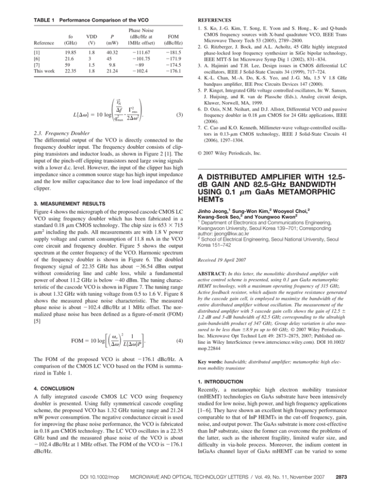
TABLE 1 Performance Comparison of the VCO REFERENCES Reference fo (GHz) VDD (V) P (mW) Phase Noise (dBc/Hz at 1MHz offset) FOM (dBc/Hz) [1] [6] [7] This work 19.85 21.6 59 22.35 1.8 3 1.5 1.8 40.32 45 9.8 21.24 ⫺111.67 ⫺101.75 ⫺89 ⫺102.4 ⫺181.5 ⫺171.9 ⫺174.5 ⫺176.1 冢 冣 ıN2 2 ⌬f ⌫rms L兵⌬ 其 ⫽ 10 log 2 䡠 . qmax 2⌬2 (3) 2.3. Frequency Doubler The differential output of the VCO is directly connected to the frequency doubler input. The frequency doubler consists of clipping transistors and inductor loads, as shown in Figure 2 [1]. The input of the pinch-off clipping transistors need large swing signals with a lower d.c. level. However, the input of the clipper has high impedance since a common source stage has high input impedance and the low miller capacitance due to low load impedance of the clipper. 3. MEASUREMENT RESULTS Figure 4 shows the micrograph of the proposed cascode CMOS LC VCO using frequency doubler which has been fabricated in a standard 0.18 m CMOS technology. The chip size is 653 ⫻ 715 m2 including the pads. All measurements are with 1.8 V power supply voltage and current consumption of 11.8 mA in the VCO core circuit and frequency doubler. Figure 5 shows the output spectrum at the center frequency of the VCO. Harmonic spectrum of the frequency doubler is shown in Figure 6. The doubled frequency signal of 22.35 GHz has about ⫺36.54 dBm output without considering line and cable loss, while a fundamental power of about 11.2 GHz is below ⫺40 dBm. The tuning characteristic of the cascode VCO is shown in Figure 7. The tuning range is about 1.32 GHz with tuning voltage from 0.5 to 1.6 V. Figure 8 shows the measured phase noise characteristic. The measured phase noise is about ⫺102.4 dBc/Hz at 1 MHz offset. The normalized phase noise has been defined as a figure-of-merit (FOM) [5] FOM ⫽ 10 log 冋冉 冊 册 o 2 1 . ⌬ L兵⌬其P (4) The FOM of the proposed VCO is about ⫺176.1 dBc/Hz. A comparison of the CMOS LC VCO based on the FOM is summarized in Table 1. 1. S. Ko, J.-G. Kim, T. Song, E. Yoon and S. Hong., K- and Q-bands CMOS frequency sources with X-band quadrature VCO, IEEE Trans Microwave Theory Tech 53 (2005), 2789 –2800. 2. G. Ritzberger, J. Bock, and A.L. Acholtz, 45 GHz highly integrated phase-locked loop frequency synthesizer in SiGe bipolar technology, IEEE MTT-S Int Microwave Symp Dig 1 (2002), 831– 834. 3. A. Hajimiri and T.H. Lee, Design issues in CMOS differential LC oscillators, IEEE J Solid-State Circuits 34 (1999), 717–724. 4. K.-L. Chan, M.-A. Do, K.-S. Yeo, and J.-G. Ma, 1.5 V 1.8 GHz bandpass amplifier, IEE Proc Circuits Devices 147 (2000). 5. P. Kinget, Integrated GHz voltage controlled oscillators, In: W. Sansen, J. Huijsing, and R. van de Plassche (Eds.), Analog circuit design, Kluwer, Norwell, MA, 1999. 6. D. Ozis, N.M. Neihart, and D.J. Allstot, Differential VCO and passive frequency doubler in 0.18 m CMOS for 24 GHz applications, IEEE (2006). 7. C. Cao and K.O. Kenneth, Millimeter-wave voltage-controlled oscillators in 0.13-m CMOS technology, IEEE J Solid-State Circuits 41 (2006), 1297–1304. © 2007 Wiley Periodicals, Inc. A DISTRIBUTED AMPLIFIER WITH 12.5dB GAIN AND 82.5-GHz BANDWIDTH USING 0.1 m GaAs METAMORPHIC HEMTs Jinho Jeong,1 Sung-Won Kim,2 Wooyeol Choi,2 Kwang-Seok Seo,2 and Youngwoo Kwon2 1 Department of Electronics and Communications Engineering, Kwangwoon University, Seoul Korea 139 –701; Corresponding author: jjeong@kw.ac.kr 2 School of Electrical Engineering, Seoul National University, Seoul Korea 151–742 Received 19 April 2007 ABSTRACT: In this letter, the monolithic distributed amplifier with active control scheme is presented, using 0.1 m GaAs metamorphic HEMT technology, with a maximum operating frequency of 315 GHz. Active feedback resistor, which adjusts the negative resistance generated by the cascode gain cell, is employed to maximize the bandwidth of the entire distributed amplifier without oscillation. The measurement of the distributed amplifier with 5 cascode gain cells shows the gain of 12.5 ⫾ 1.2 dB and 3-dB bandwidth of 82.5 GHz corresponding to the ultrahigh gain-bandwidth product of 347 GHz. Group delay variation is also measured to be less than ⫾8.9 ps up to 60 GHz. © 2007 Wiley Periodicals, Inc. Microwave Opt Technol Lett 49: 2873–2875, 2007; Published online in Wiley InterScience (www.interscience.wiley.com). DOI 10.1002/ mop.22844 Key words: bandwidth; distributed amplifier; metamorphic high electron mobility transistor 1. INTRODUCTION 4. CONCLUSION A fully integrated cascode CMOS LC VCO using frequency doubler is presented. Using fully symmetrical cascode coupling scheme, the proposed VCO has 1.32 GHz tuning range and 21.24 mW power consumption. The negative conductance circuit is used for improving the phase noise performance, the VCO is fabricated in 0.18 m CMOS technology. The LC VCO oscillates in a 22.35 GHz band and the measured phase noise of the VCO is about ⫺102.4 dBc/Hz at 1 MHz offset. The FOM of the VCO is ⫺176.1 dBc/Hz. DOI 10.1002/mop Recently, a metamorphic high electron mobility transistor (mHEMT) technologies on GaAs substrate have been intensively studied for low noise, high power, and high frequency applications [1– 6]. They have shown an excellent high frequency performance comparable to that of InP HEMTs in the cut-off frequency, gain, noise, and output power. The GaAs substrate is more cost-effective than InP substrate, since the former can overcome the problems of the latter, such as the inherent fragility, limited wafer size, and difficulty in via-hole process. Moreover, the indium content in InGaAs channel layer of GaAs mHEMT can be varied to some MICROWAVE AND OPTICAL TECHNOLOGY LETTERS / Vol. 49, No. 11, November 2007 2873 extent to optimize its performance depending on the applications [1]. Therefore, GaAs mHEMTs are suitable for low-cost high performance millimeter-wave ICs in spite of its low on-state breakdown voltage and poor thermal conductivity of GaAs substrate [2], such as ultralow noise amplifiers [3], power amplifiers [4], high order frequency dividers [5], and broadband distributed amplifiers [2, 6]. In this article, a cascode distributed amplifier with ultrahigh gain-bandwidth product of 347 GHz is presented, using 0.1 m GaAs mHEMT technologies, for high-speed fiber optic communications. We believe this result belongs to one of the highest gain-bandwidth products among the reported distributed amplifier using GaAs mHEMT technologies. The active feedback resistors were employed at the cascode gain FET to optimize the bandwidth and stability of the distributed amplifier, which was previously proposed by the authors in Ref. 7. Therefore, this work demonstrates that the combination of high performance GaAs mHEMT technology and the proposed active control scheme can result in the ultrahigh gain-bandwidth product of the distributed amplifier. 2. DESIGN OF CASCODE DISTRIBUTED AMPLIFIER Cascode FETs are widely used as a gain cell for a broadband distributed amplifier, since they provide a high gain at high frequency resulting in high gain-bandwidth product [2, 6, 7]. They also present the negative resistance compensating for the losses caused by resistive components in FETs and transmission lines, which further improves the high frequency performance and bandwidth of distributed amplifier. However, it sometimes causes the instability at the high-frequency band edge because of overcompensation or excessively generated negative resistance. The feedback resistor is usually employed at the gate of CG-FET to stabilize the cascode FETs by reducing the amount of negative resistance. However, excessive feedback resistance rather degrades the high frequency performance of cascode FETs resulting in the bandwidth reduction of distributed amplifier. Therefore, the value of this feedback resistance should be accurately determined for trade-off between stability and bandwidth. But, it is difficult to find the optimum feedback resistance value at the design stage because of the process variations and inaccurate device models especially at high frequencies [7]. In this work, the fixed thin film resistor at the gate of CG-FET of cascode FET was replaced with active variable resistor, so that Figure 2 Photograph of the fabricated distributed amplifier. The chip size is 1.7 mm ⫻ 0.9 mm. [Color figure can be viewed in the online issue, which is available at www.interscience.wiley.com] its value can be adjusted after chip fabrication as shown in Figure 1 [7]. Figure 1 shows the circuit schematic of 5-stage distributed amplifier using cascode FETs with active feedback resistors at the gate of CF-FETs. Two 80 m-wide FETs are used for cascode configuration. The active feedback resistors are implemented with the channel resistance of 50 m-wide FET biased at linear region. The feedback resistance can be controlled by the gate-to-source or gate-to-drain bias voltage Vfc, which determines the negative resistance generated by cascode FET. Therefore, it can effectively optimize the high frequency performance of distributed amplifier after MMIC fabrication. The big parallel resistor Rp was used to make sure that the drain and source of FET have the same bias voltage. It also helps the variable resistor to operate in the linear region with the large input signal. ⟨ scalable large-signal model was developed based on the measured S-parameters and DC IV characteristics of 100 m-wide FETs. The coefficients of the nonlinear drain current and capacitance equations were optimized to best curve fit the measured data at various gate and drain bias region. The CPW lines with impedance of 70 ohm were used for the gate and drain transmission lines. The gate and drain line impedance is reduced close to 50 ohm as a result of the loading effect by the input and output capacitance of FET. The gate and drain termination impedance, Rgt and Rdt, were implemented with the thin film resistor of 50 ohm. Air bridges are placed around tee junctions to minimize the discontinuities. The open stub was added at the input port to improve the input return loss at high frequency. 3. FABRICATION AND MEASUREMENT Figure 1 Circuit schematic of the designed distributed amplifier with 5 cascode gain cells 2874 A designed distributed amplifier was fabricated using In0.4AlAs/ In0.35GaAs metamorphic HEMTs, which were grown by molecular beam epitaxy on semi-insulating GaAs substrate. The measurement of the 0.1 m GaAs mHEMTs showed the current gain cut-off frequency of 153 GHz and the maximum operating frequency of 315 GHz at the gate bias voltage of 0.1 V and drain bias voltage of 2 V. The maximum available gain was higher than 10 dB at 77 GHz. The gate breakdown voltage was measured to be 7.1 V with gate leakage current of 1 mA/mm [8]. Figure 2 shows the fabricated distributed amplifier on CPW, so that there is no need for via-hole process. The thickness of GaAs substrate was 650 m. The chip size is as small as 1.7 ⫻ 0.9 mm2. The S-parameters were measured up to 110 GHz by on-wafer probing as shown in Figure 3. The bias condition was as follows: the gate bias voltage of common-source FET, Vg1 ⫽ ⫺0.35 V, the gate bias voltage of common-gate FET, Vg2 ⫽ 0.9 V, and the drain bias voltage, Vd ⫽ 3.3 V. The Vg1 and Vd were applied through the MICROWAVE AND OPTICAL TECHNOLOGY LETTERS / Vol. 49, No. 11, November 2007 DOI 10.1002/mop external bias tees. The total DC current was 128 mA, including the current of 66 mA flowing into the drain termination resistor Rdt of 50 ohm. The feedback control voltage Vfc, which determines the gate feedback resistance of cascode FET, was adjusted to obtain the optimum performance of distributed amplifier. As shown in Figure 3, the measurement shows the gain of 12.5 ⫾ 1.2 dB with 3-dB bandwidth of 82.5 GHz at Vfc of 0.0 V, which corresponds to gain-bandwidth product of 347 GHz. The input and output return losses were better than 10 dB up to 50 GHz, and 8 dB up to 80 GHz. This figure also demonstrates that the bandwidth and stability of the distributed amplifier can be controlled by Vfc. At Vfc greater than 0.4 V, the gain overshoot was observed together with S22 higher than zero at high frequency band edge. It implies that the cascode distributed amplifier can be instable especially at high frequency band edge because of the excessively generated negative resistance by cascode FET [7]. Therefore, the active feedback control is an effective way to tune the performance of the GaAs mHEMT distributed amplifier, as well for maximum gain-bandwidth product without oscillation. Group delay variation, which is related to the phase linearity of the amplifier, was also measured at Vfc ⫽ 0.0 V, or the control voltage allowing the best gainbandwidth product. Figure 4 shows the group delay variation less than ⫾8.9 ps up to 60 GHz. Figure 4 0.0 V Measured group delay at the feedback control voltage Vfc ⫽ ACKNOWLEDGMENT 4. CONCLUSION In this article, the monolithic distributed amplifier with high gainbandwidth product was presented using 0.1 m GaAs mHEMT technology on coplanar waveguide. A 5-stage cascode distributed amplifier showed the gain-bandwidth product of 347 GHz with group delay variation less than ⫾8.9 ps up to 60 GHz. It is also shown that the active feedback resistors employed in the cascode gain cell can effectively adjust the bandwidth and stability of the distributed amplifier after chip fabrication. Therefore, it can minimize the failure of the monolithic distributed amplifiers, such as oscillation at high frequency band edge, which may be caused because of the inaccurate device model and process variations. It is worthwhile to note that the developed GaAs mHEMT distributed amplifier with the active control scheme in this work is useful for low-cost high-speed optical communications. This work was financially supported by the National Program for Tera-Hz Level Integrated Circuits of the Minister of Science and Technology as one of the 21 Century Frontier Programs. REFERENCES 1. P.M. Smith, D. Duga, K. Chu, K. Nichols, K.G. Duh, J. Fisher, L. MtPleasant, D. Xu, L. Gunter, A. Vera, R. Lender, and D. Meharry, Progress in GaAs Metamorphic HEMT Technology for microwave applications, IEEE GaAs IC Dig (2003), 21–24. 2. M.S. Heins, C.F. Campbell, M-Y. Kao, M.E. Muir, and J.M. Carroll, A GaAs MHEMT distributed amplifier with 300-GHz gain-bandwidth product for 40-Gb/s optical applications, IEEE MTT-S Dig, Seattle, WA (2002), 1061–1064. 3. A. Tessmann, A. Leuther, C. Schwoerer, H. Massler, S. Kudszus, W. Reinert, and M. Schlechtweg, A coplanar 94 GHz low-noise amplifier MMIC using 0.07 m Metamorphic Cascode HEMTs, IEEE MTT-S, Philadelphia, PA (2003), 1581–1584. 4. K.J. Herrick, K.W. Brown, F.A. Rose, C.S. Whelan, J. Kotce, J.R. Laroche, and Y. Zhang, W-band Metamorphic HEMT with 267 mW output power, IEEE MTT-S, Long Beach, CA (2005), 843– 846. 5. J. Jeong, S.-W. Kim, W. Choi, H. Noh, K.-M. Lee, K. Seo, and Y. Kwon, W-Band divide-by-3 frequency divider using 0.1 m InAlAs/ InGaAs Metamorphic HEMT Technology, IEE Electron Lett 41 (2005), 1005–1006. 6. G. Wolf, H. Happy, S. Demichel, R. Leblanc, F. Blache, R. Lefevre, and G. Dambrine, A Metamorphic GaAs HEMT distributed amplifier with 50-GHz bandwidth and low noise for 40 Gbits/s, IEEE MTT-S, Long Beach, CA (2005), 2231–2233. 7. J. Jeong and Y. Kwon, Monolithic distributed amplifier with active control schemes for optimum gain and group delay flatness, bandwidth and stability, IEEE Trans Microwave Theory Tech 52 (2004), 1101– 1110. 8. S.-W. Kim, K.-M. Lee, J.-H. Lee, and K.-S. Seo, High-performance 0.1 m In0.4AlAs/In0.35GaAs MHEMTs with Ar plasma treatment, IEEE Electron Device Lett 26 (2005), 787–789. © 2007 Wiley Periodicals, Inc. Figure 3 Measured S-parameters at various feedback control voltage Vfc with Vg1 ⫽ ⫺0.35 V, Vg2 ⫽ 0.9 V, and Vd ⫽ 3.3 V. The S11 and S22 were measured at Vfc ⫽ 0.0 V DOI 10.1002/mop MICROWAVE AND OPTICAL TECHNOLOGY LETTERS / Vol. 49, No. 11, November 2007 2875


