APPLICATION NOTE
Gain Block Bias Networks
Introduction
Skyworks gain block amplifiers are InGaP/GaAs HBT integrated
circuits. They use a Darlington-pair transistor configuration with
bias and feedback resistors properly selected to determine the
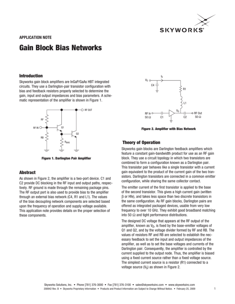
gain, input and output impedances and bias parameters. A schematic representation of the amplifier is shown in Figure 1.
IS
VS
C4
R1
L1
RF OUT
RF In
50 Ω
RF
Q1
RF IN
VD
C1
C2
RF Out
50 Ω
Figure 2. Amplifier with Bias Network
Q2
RB
RBIAS
Figure 1. Darlington Pair Amplifier
Abstract
As shown in Figure 2, the amplifier is a two-port device. C1 and
C2 provide DC blocking in the RF input and output paths, respectively. RF ground is made through the remaining package pins.
The RF output port is also used to provide bias to the amplifier
through an external bias network (C4, R1 and L1). The values
of the bias decoupling network components are selected based
upon the frequency of operation and supply voltage available.
This application note provides details on the proper selection of
these components.
Theory of Operation
Skyworks gain blocks are Darlington feedback amplifiers which
feature a constant gain-bandwidth product for use as an RF gain
block. They use a circuit topology in which two transistors are
combined to form a configuration known as a Darlington pair.
This transistor pair behaves like a single transistor with a current
gain equivalent to the product of the current gain of the two transistors. Darlington transistors are connected in a common emitter
configuration, while sharing the same collector contact.
The emitter current of the first transistor is applied to the base
of the second transistor. This gives a high current gain (written
b or Hfe), and takes less space than two discrete transistors in
the same configuration. As RF gain blocks, Darlington pairs are
offered as integrated packaged devices, usable from very low
frequency to over 10 GHz. They exhibit good broadband matching
into 50 W and tight performance distributions.
The designed DC voltage that appears at the RF output of the
amplifier, known as VD, is fixed by the base-emitter voltages of
Q1 and Q2, and by the voltage divider formed by RF and RB. The
values of resistors RF and RB are selected to establish the necessary feedback to set the input and output impedances of the
amplifier, as well as to set the base voltages and currents of the
Darlington pair. Consequently, the amplifier is controlled by the
current supplied to the output node. Thus, the amplifier is biased
using a fixed current source rather than a fixed voltage source.
The simplest current source is a resistor (R1) connected to a
voltage source (VS) as shown in Figure 2.
Skyworks Solutions, Inc. • Phone [781] 376-3000 • Fax [781] 376-3100 • sales@skyworksinc.com • www.skyworksinc.com
200942 Rev. B • Skyworks Proprietary Information • Products and Product Information are Subject to Change Without Notice. • February 25, 2009
1
APPLICATION NOTE • Gain Block Bias Networks
Figure 3 shows a simplified DC equivalent circuit of the Darlington
pair gain block. The voltage that appears at the point labeled VD,
which is the RF output of the amplifier, is the series sum of the
forward voltages of the base-emitter junctions of the transistors
and the voltage drop across RF. The forward voltage of each of
the base-emitter diodes is exponentially related to the current
flowing through them, and is also affected by temperature.
Skyworks offers a series of gain block amplifiers in 3 different
package styles (see Figure 4). These products differ by such
parameters as gain, output power, frequency range and supply
current draw, among others. Proper selection of a gain block
depends upon the specific requirements of the application. Table
1 shows a list of gain blocks currently offered.
Since the current through each of the base-emitter diodes directly
controls the collector current for each of these transistors (these
paths are not shown in this diagram), it is clearly important to
control the bias current through each of the base-emitter junctions with a well-regulated current source. If a regulated voltage
source is connected to the VD point in place of current source, the
current through the transistors in the amplifier can vary widely
in response to comparatively small changes in supply voltage.
Additionally, due to the I-V characteristics of the base-emitter
junction of each transistor, a small change in voltage or temperature can result in a large change in current.
NOTE: For purposes of this application note, the SKY65015-92LF
will be referenced. The information provided is common to
other Skyworks gain block part numbers. Refer to the data
sheets for specific part information.
VD
RF
VBE
Q1
RB
RBIAS
VBE
Q2
Figure 4. Gain Block Package Styles
Figure 3. Simplified DC Equivalent Circuit of
Darlington Pair Gain Block
2
Skyworks Solutions, Inc. • Phone [781] 376-3000 • Fax [781] 376-3100 • sales@skyworksinc.com • www.skyworksinc.com
February 25, 2009 • Skyworks Proprietary Information • Products and Product Information are Subject to Change Without Notice. • 200942 Rev. B
APPLICATION NOTE • Gain Block Bias Networks
Table 1. Skyworks Gain Block Part List
Test
Frequency
(GHz)
Gain
Typ.
(dB)
Quiescent
Current
Typ.
(mA)
VCC
(V)
Noise Figure
Typ.
(dB)
OIP3
(dBm)
P1 dB
(dBm)
Part Number
Package
Frequency
Range
(GHz)
SKY65013-70LF
SOT-89
LF-7
2
12.5
40
5
5.5
29
12.5
SKY65014-70LF
SOT-89
LF-6
2
16
70
5
4.8
36
18
SKY65015-70LF
SOT-89
LF-6
2
18
70
5
4.2
35
17
SKY65016-70LF
SOT-89
LF-3
2
20
40
5
4.8
27
14
SKY65017-70LF
SOT-89
LF-6
2
20
100
5
4.5
35
20
SKY65013-92LF
SC-88
LF-12
2
12.5
40
5
5.8
29
12.5
SKY65014-92LF
SC-88
LF-9
2
15
70
5
5.4
36
15
SKY65015-92LF
SC-88
LF-6
2
18
70
5
4.8
35
18
SKY65016-92LF
SC-88
LF-3
2
20
40
5
5.4
27
20
SKY65013-214LF
Micro-X
LF-6
2
11.5
40
5
5.4
29
11.5
SKY65014-214LF
Micro-X
LF-6
2
13.5
70
5
4.6
36
13.5
SKY65015-214LF
Micro-X
LF-6
2
16
70
5
5.2
24
16
SKY65016-214LF
Micro-X
LF-3
2
19
40
5
6.5
20
19
The selection of inductor, L1 is based upon its self-resonant
frequency (SRF) and its impedance in the band of operation (Fo).
The inductor’s SRF should be greater than Fo and its impedance
value should be approximately 10 times greater than Zo (50 W).
Table 3 shows values for inductor L1 based upon the frequency
of operation.
The bill of materials for operation at 2 GHz for the SKY65015-92LF
gain block amplifier circuit as shown in Figure 2 is shown in Table
2. Capacitors C1 and C2 are selected to provide DC blocking for
the RF input and output. Capacitor C4 is used for a bias decoupling
capacitor. This capacitor provides suppression of low frequency RF
signals appearing across the DC bias lines.
Table 2. SKY65015-92LF Bill of Materials
Part
ID
Description
Qty.
Size
1
C1, C2, C4
Capacitor
3
0603
2
L1
Inductor
1
0603
3
R1
Resistor
1
0603
Value
Units
Product Number
47
nF
GRM188R71E473K
Murata
33
nH
0603CS-33NX_LU
CoilCraft
W
Manufacturer
See Current Limiting Res. Table
Skyworks Solutions, Inc. • Phone [781] 376-3000 • Fax [781] 376-3100 • sales@skyworksinc.com • www.skyworksinc.com
200942 Rev. B • Skyworks Proprietary Information • Products and Product Information are Subject to Change Without Notice. • February 25, 2009
3
APPLICATION NOTE • Gain Block Bias Networks
Table 3. Recommended Chokes by Application Band
Frequency(1)
(GHz)
Inductance
(nH)
SRF(2)
(GHz)
Impedance
(XL)(3)
Mfg. Part Number
Manufacturer
0.4
220
0.82
553
0805CS-221X_L_
CoilCraft
0.8
120
1.10
603
0805CS-121X_L_
CoilCraft
0.9
110
1.10
622
0805CS-111X_L_
CoilCraft
1.2
91
1.33
686
0805CS-910X_L_
CoilCraft
1.6
47
1.70
472
0805CS-470X_L_
CoilCraft
1.8
56
1.90
633
0603CS-56NX_L_
CoilCraft
1.9
47
2.00
561
0603CS-47NX_L_
CoilCraft
2.1
39
2.20
514
0603CS-39NX_L_
CoilCraft
2.2
33
2.30
456
0603CS-33NX_L_
CoilCraft
2.4
27
2.80
407
0603CS-27NX_L_
CoilCraft
3
22
4.60
414
LQW18AN22NJ00
Murata
3.6
22
4.60
497
LQW18AN22NJ00
Murata
4.2
22
4.60
580
LQW18AN22NJ00
Murata
4.9
18
5.50
554
LQW18AN18NJ00
Murata
6
15
6.00
565
LQW18AN15NJ00
Murata
1. Evaluation board L1 nominal value = 33 nH (2.2 GHz). At high microwave frequencies, where no lumped element inductors are available, a ¼ wave length line with a stub may be used.
2. Self-resonant frequency
3. Choke selection is based upon SRF > FO and impedance (XL = 2*p*F*L) value 10 times greater than ZO (50 W). For extreme wideband operation 2 chokes may be combined, i.e. (33 nH and 110 nH).
In most electronic systems, the power supply produces a fixed
voltage, rather than a fixed current to the devices comprising the
system. The selection of R1 is based upon the system supply
voltage available and the value of VD that occurs when the correct supply DC current is present, as well as the power dissipated
by the resistor. The resistor value is derived from the following
equation: R = (VS-VD)/IS. The minimum resistor power dissipation
rating is based upon the power dissipated across the resistor
(Pdiss = V2 * R1). It is recommended to use resistors rated for at
least twice the calculated value of Pdiss; otherwise, use parallel
or a series split of several resistors that are each easily capable
of dissipating their dissipated power levels. For the evaluation
circuit as supplied by Skyworks, the default resistor size is ‘0603’
with a power rating of 1000 mW. Check the manufacturer’s
power rating when using smaller sized resistors.
Table 4. Current Limiting Resistor Values
VS (V)
R1 Resistance (W)
Mimimum Resistor Power
Dissipation Rating (mW)
Product Number
Manufacturer
4.4
0.5(1)
–
ERJ-3GEY0R00V
Panasonic
5
8.2
125
ERJ-3GEYJ8R2V
Panasonic
6
24
250
ERJ-3GEYJ240V
Panasonic
7
36
500
ERJ-3GEYJ360V
Panasonic
8
51
500
ERJ-3GEYJ510V
Panasonic
9
68
1000
ERJ-3GEYJ680V
Panasonic
10
82
1000
ERJ-3GEYJ820V
Panasonic
12
110
1000
ERJ-3GEYJ111V
Panasonic
1. At VS = 4.4 V, the series resistance (R1) is the DC resistance of the bias inductors
(L1, L2 and L3) and trace lines.
4
Skyworks Solutions, Inc. • Phone [781] 376-3000 • Fax [781] 376-3100 • sales@skyworksinc.com • www.skyworksinc.com
February 25, 2009 • Skyworks Proprietary Information • Products and Product Information are Subject to Change Without Notice. • 200942 Rev. B
APPLICATION NOTE • Gain Block Bias Networks
Low Frequency Operation
No L2, L3
19
S21 (dB)
18
The modified bill of materials for extreme low frequency performance of the SKY65015-92LF is shown in Table 5. Gain (|S21|)
performance using the bill of materials from Table 2 and Table 5
is shown in Figure 6. The ferrite bead and inductor L3 improve
the frequency response below 300 MHz and reduce the variation
in bias current, at the cost of degraded performance at 1 GHz
and the monetary cost of the components themselves.
17
16
15
14
0
1
2
3
4
5
6
Frequency (GHz)
Figure 6. SKY65015-92LF S21 vs.
Frequency, IS =70 mA, TA = 25 °C
IS
VS
With L2 Ferrite
20
For operation with signals below 300 MHz, Ferrite Bead (L2) and
Inductor (L3) may be added. Figure 5 shows the schematic for
low frequency applications below 300 MHz. Resistor R1 must
also be added in series with the inductors to limit the power
supply current when the power supply provides a constant
voltage, as discussed above.
L2
C4
L3
R1
L1
VD
Input
C1
Output
C2
Figure 5. Amplifier with Low Frequency Bias Network
Table 5. SKY65015-92LF Bill of Materials for Low Frequency Applications
Part
ID
Description
Qty.
Size
Value
Units
Product Number
Manufacturer
1
C1, C2, C4
Capacitor
3
0603
47
nF
GRM188R71E473K
Murata
2
L1
Inductor
1
0603
33
nH
0603CS-33NX_LU
CoilCraft
3
L2
Ferrite Bead
1
1810
1600
W
FBMH4525HM162N-T
Taiyo-Yuden
4
L3
Inductor
1
0805
110 nH
nH
0805CS-111X_L_
CoilCraft
5
R1
Resistor
1
0603
Summary
Skyworks gain block amplifiers are InGaP/GaAs HBT integrated
circuits using the Darlington-pair transistor configuration which
requires a constant DC current applied to the output port to bias
the device. Factors such as voltage supply level, system characteristic impedance, frequency of operation and cost should
W
See Current Limiting Res. Table
be taken into account when selecting the proper DC current
limiting and RF decoupling bias components and RF DC blocking
components in the signal path. The information provided in this
application note addresses these tasks. Further information about
specific gain block amplifiers may be found in the appropriate
data sheets at www.skyworksinc.com.
Skyworks Solutions, Inc. • Phone [781] 376-3000 • Fax [781] 376-3100 • sales@skyworksinc.com • www.skyworksinc.com
200942 Rev. B • Skyworks Proprietary Information • Products and Product Information are Subject to Change Without Notice. • February 25, 2009
5
APPLICATION NOTE • Gain Block Bias Networks
Copyright © 2008, 2009, Skyworks Solutions, Inc. All Rights Reserved.
Information in this document is provided in connection with Skyworks Solutions, Inc. (“Skyworks”) products or services. These materials, including the information contained herein, are provided
by Skyworks as a service to its customers and may be used for informational purposes only by the customer. Skyworks assumes no responsibility for errors or omissions in these materials or the
information contained herein. Skyworks may change its documentation, products, services, specifications or product descriptions at any time, without notice. Skyworks makes no commitment to
update the materials or information and shall have no responsibility whatsoever for conflicts, incompatibilities, or other difficulties arising from any future changes.
No license, whether express, implied, by estoppel or otherwise, is granted to any intellectual property rights by this document. Skyworks assumes no liability for any materials, products or
information provided hereunder, including the sale, distribution, reproduction or use of Skyworks products, information or materials, except as may be provided in Skyworks Terms and
Conditions of Sale.
THE MATERIALS, PRODUCTS AND INFORMATION ARE PROVIDED “AS IS” WITHOUT WARRANTY OF ANY KIND, WHETHER EXPRESS, IMPLIED, STATUTORY, OR OTHERWISE, INCLUDING FITNESS FOR A
PARTICULAR PURPOSE OR USE, MERCHANTABILITY, PERFORMANCE, QUALITY OR NON-INFRINGEMENT OF ANY INTELLECTUAL PROPERTY RIGHT; ALL SUCH WARRANTIES ARE HEREBY EXPRESSLY
DISCLAIMED. SKYWORKS DOES NOT WARRANT THE ACCURACY OR COMPLETENESS OF THE INFORMATION, TEXT, GRAPHICS OR OTHER ITEMS CONTAINED WITHIN THESE MATERIALS. SKYWORKS
SHALL NOT BE LIABLE FOR ANY DAMAGES, INCLUDING BUT NOT LIMITED TO ANY SPECIAL, INDIRECT, INCIDENTAL, STATUTORY, OR CONSEQUENTIAL DAMAGES, INCLUDING WITHOUT LIMITATION,
LOST REVENUES OR LOST PROFITS THAT MAY RESULT FROM THE USE OF THE MATERIALS OR INFORMATION, WHETHER OR NOT THE RECIPIENT OF MATERIALS HAS BEEN ADVISED OF THE
POSSIBILITY OF SUCH DAMAGE.
Skyworks products are not intended for use in medical, lifesaving or life-sustaining applications, or other equipment in which the failure of the Skyworks products could lead to personal injury,
death, physical or environmental damage. Skyworks customers using or selling Skyworks products for use in such applications do so at their own risk and agree to fully indemnify Skyworks for any
damages resulting from such improper use or sale.
Customers are responsible for their products and applications using Skyworks products, which may deviate from published specifications as a result of design defects, errors, or operation of
products outside of published parameters or design specifications. Customers should include design and operating safeguards to minimize these and other risks. Skyworks assumes no liability for
applications assistance, customer product design, or damage to any equipment resulting from the use of Skyworks products outside of stated published specifications or parameters.
Skyworks, the Skyworks symbol, and “Breakthrough Simplicity” are trademarks or registered trademarks of Skyworks Solutions, Inc., in the United States and other countries. Third-party brands
and names are for identification purposes only, and are the property of their respective owners. Additional information, including relevant terms and conditions, posted at www.skyworksinc.com, are
incorporated by reference.
6
Skyworks Solutions, Inc. • Phone [781] 376-3000 • Fax [781] 376-3100 • sales@skyworksinc.com • www.skyworksinc.com
February 25, 2009 • Skyworks Proprietary Information • Products and Product Information are Subject to Change Without Notice. • 200942 Rev. B
