Quad Voltage Monitor and Sequencer
ADM1185
FEATURES
FUNCTIONAL BLOCK DIAGRAM
VCC
Powered from 2.7 V to 5.5 V on the VCC pin
Monitors 4 supplies via 0.8% accurate comparators
Logical core with internal timeouts provides power supply
sequencing and fault protection
4 inputs can be programmed to monitor different voltage
levels with resistor dividers
3 open-drain enable outputs
Open-drain power-good output (PWRGD)
10-lead MSOP
VIN1
APPLICATIONS
VIN3
ADM1185
POWER AND REF = 0.6V
REFERENCE
GENERATOR
OUT1
REF = 0.6V
OUT2
VIN2
REF = 0.6V
STATE
MACHINE
CORE
OUT3
REF = 0.6V
Monitor and alarm functions
Power supply sequencing
Telecommunication and data communication equipment
PCs/servers
PWRGD
VIN4
REF = 0.6V
06196-001
GND
Figure 1.
GENERAL DESCRIPTION
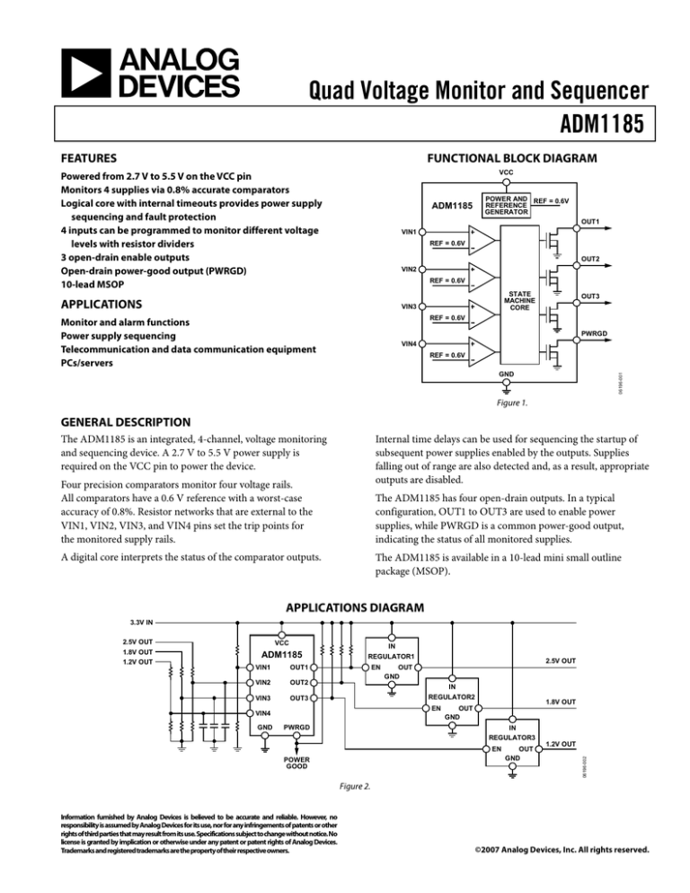
The ADM1185 is an integrated, 4-channel, voltage monitoring
and sequencing device. A 2.7 V to 5.5 V power supply is
required on the VCC pin to power the device.
Internal time delays can be used for sequencing the startup of
subsequent power supplies enabled by the outputs. Supplies
falling out of range are also detected and, as a result, appropriate
outputs are disabled.
Four precision comparators monitor four voltage rails.
All comparators have a 0.6 V reference with a worst-case
accuracy of 0.8%. Resistor networks that are external to the
VIN1, VIN2, VIN3, and VIN4 pins set the trip points for
the monitored supply rails.
The ADM1185 has four open-drain outputs. In a typical
configuration, OUT1 to OUT3 are used to enable power
supplies, while PWRGD is a common power-good output,
indicating the status of all monitored supplies.
A digital core interprets the status of the comparator outputs.
The ADM1185 is available in a 10-lead mini small outline
package (MSOP).
APPLICATIONS DIAGRAM
3.3V IN
VCC
ADM1185
VIN1
OUT1
VIN2
OUT2
VIN3
OUT3
IN
REGULATOR1
EN
IN
REGULATOR2
EN
VIN4
GND
2.5V OUT
OUT
GND
PWRGD
1.8V OUT
OUT
GND
IN
REGULATOR3
EN
POWER
GOOD
OUT
GND
1.2V OUT
06196-002
2.5V OUT
1.8V OUT
1.2V OUT
Figure 2.
Information furnished by Analog Devices is believed to be accurate and reliable. However, no
responsibility is assumed by Analog Devices for its use, nor for any infringements of patents or other
rights of third parties that may result from its use. Specifications subject to change without notice. No
license is granted by implication or otherwise under any patent or patent rights of Analog Devices.
Trademarks and registered trademarks are the property of their respective owners.
©2007 Analog Devices, Inc. All rights reserved.
ADM1185
SPECIFICATIONS
VCC = 2.7 V to 5.5 V, TA = −40°C to +85°C, unless otherwise noted.
Table 1.
Parameter
VCC PIN
Operating Voltage Range, VCC
Supply Current, IVCC
VIN1 TO VIN4 (VINx) PINS
Input Current, IVINLEAK
Input Rising Threshold, VTHR
Min
Typ
Max
Unit
2.7
3.3
24
5.5
80
V
μA
+20
0.604
8
nA
V
VVINx = 0.7 V
0.600
0
0.4
0.4
+1
V
V
μA
V
VCC = 2.7 V, ISINK = 2 mA
VCC = 1 V, ISINK = 100 μA
−20
0.595
2
OUT1 TO OUT3 (OUTx), PWRGD PINS
Output Low Voltage, VOUTL
Leakage Current, IALERT
VCC that Guarantees Valid Outputs
−1
1
ms
ms
All outputs are guaranteed to be either low or giving
a valid output level from VCC = 1 V
Delays only applicable to certain operations states;
refer to state diagram (Figure 19) for more details
VCC = 3.3 V, see Figure 7
VCC = 3.3 V, see Figure 7
μs
μs
VCC = 3.3 V, see Figure 9
VCC = 3.3 V, see Figure 10
TIMING DELAYS
VIN1 to OUT1 Rising Delay
VIN4 to PWRGD Rising Delay
VIN2 to OUT2, VIN3 to OUT3
Low-to-High Propagation Delay
High-to-Low Propagation Delay, All Inputs
100
100
190
190
280
280
30
30
Page 3 of 16
Conditions
ADM1185
ABSOLUTE MAXIMUM RATINGS
TA = 25°C, unless otherwise noted.
THERMAL RESISTANCE
Table 2.
θJA is specified for the worst-case conditions, that is, a device
soldered in a circuit board for surface-mount packages.
Parameter
VCC Pin
VINx Pins
OUTx, PWRGD Pins
Storage Temperature Range
Operating Temperature Range
Lead Temperature Soldering (10 sec)
Junction Temperature
Rating
−0.3 V to +6 V
−0.3 V to +6 V
−0.3 V to +6 V
−65°C to +125°C
−40°C to +85°C
300°C
150°C
Table 3. Thermal Resistance
Package Type
10-Lead MSOP
ESD CAUTION
Stresses above those listed under Absolute Maximum Ratings
may cause permanent damage to the device. This is a stress
rating only; functional operation of the device at these or any
other conditions above those indicated in the operational
section of this specification is not implied. Exposure to absolute
maximum rating conditions for extended periods may affect
device reliability.
Page 4 of 16
θJA
137.5
Unit
°C/W
ADM1185
OUTLINE DIMENSIONS
3.10
3.00
2.90
10
3.10
3.00
2.90
1
6
5
5.15
4.90
4.65
PIN 1
0.50 BSC
0.95
0.85
0.75
1.10 MAX
0.15
0.05
0.33
0.17
SEATING
PLANE
0.23
0.08
8°
0°
0.80
0.60
0.40
COPLANARITY
0.10
COMPLIANT TO JEDEC STANDARDS MO-187-BA
Figure 25. 10-Lead Mini Small Outline Package [MSOP]
(RM-10)
Dimensions shown in millimeters
ORDERING GUIDE
Model
ADM1185ARMZ-1 1
ADM1185ARMZ-1REEL71
EVAL-ADM1185EBZ1
1
Temperature Range
−40°C to +85°C
−40°C to +85°C
Package Description
10-Lead Mini Small Outline Package [MSOP]
10-Lead Mini Small Outline Package [MSOP]
Evaluation Board
Z = RoHS Compliant Part.
Page 13 of 16
Package Option
RM-10
RM-10
Branding
M9W
M9W


