A Σ-∆ Fractional-N Frequency Synthesizer using a
advertisement

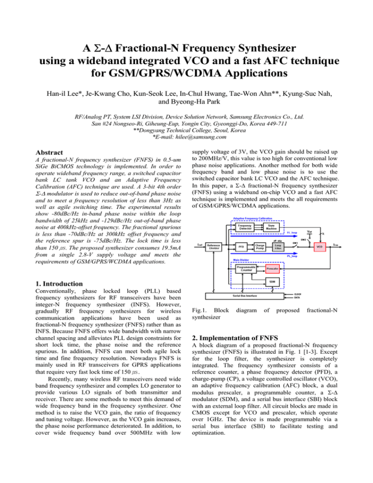
A Σ-∆ Fractional-N Frequency Synthesizer using a wideband integrated VCO and a fast AFC technique for GSM/GPRS/WCDMA Applications Han-il Lee*, Je-Kwang Cho, Kun-Seok Lee, In-Chul Hwang, Tae-Won Ahn**, Kyung-Suc Nah, and Byeong-Ha Park RF/Analog PT, System LSI Division, Device Solution Network, Samsung Electronics Co., Ltd. San #24 Nongseo-Ri, Giheung-Eup, Yongin City, Gyeonggi-Do, Korea 449-711 **Dongyang Technical College, Seoul, Korea *E-mail: hilee@samsung.com Abstract A fractional-N frequency synthesizer (FNFS) in 0.5-um SiGe BiCMOS technology is implemented. In order to operate wideband frequency range, a switched capacitor bank LC tank VCO and an Adaptive Frequency Calibration (AFC) technique are used. A 3-bit 4th order Σ-∆ modulator is used to reduce out-of-band phase noise and to meet a frequency resolution of less than 3Hz as well as agile switching time. The experimental results show -80dBc/Hz in-band phase noise within the loop bandwidth of 25kHz and -129dBc/Hz out-of-band phase noise at 400kHz-offset frequency. The fractional spurious is less than -70dBc/Hz at 300kHz offset frequency and the reference spur is -75dBc/Hz. The lock time is less than 150 ㎲. The proposed synthesizer consumes 19.5mA from a single 2.8-V supply voltage and meets the requirements of GSM/GPRS/WCDMA applications. supply voltage of 3V, the VCO gain should be raised up to 200MHz/V, this value is too high for conventional low phase noise applications. Another method for both wide frequency band and low phase noise is to use the switched capacitor bank LC VCO and the AFC technique. In this paper, a Σ-∆ fractional-N frequency synthesizer (FNFS) using a wideband on-chip VCO and a fast AFC technique is implemented and meets the all requirements of GSM/GPRS/WCDMA applications. 1. Introduction Conventionally, phase locked loop (PLL) based frequency synthesizers for RF transceivers have been integer-N frequency synthesizer (INFS). However, gradually RF frequency synthesizers for wireless communication applications have been used as fractional-N frequency synthesizer (FNFS) rather than as INFS. Because FNFS offers wide bandwidth with narrow channel spacing and alleviates PLL design constraints for short lock time, the phase noise and the reference spurious. In addition, FNFS can meet both agile lock time and fine frequency resolution. Nowadays FNFS is mainly used in RF transceivers for GPRS applications that require very fast lock time of 150 ㎲. Recently, many wireless RF transceivers need wide band frequency synthesizer and complex LO generator to provide various LO signals of both transmitter and receiver. There are some methods to meet this demand of wide frequency band in the frequency synthesizer. One method is to raise the VCO gain, the ratio of frequency and tuning voltage. However, as the VCO gain increases, the phase noise performance deteriorated. In addition, to cover wide frequency band over 500MHz with low Fig.1. Block synthesizer diagram of proposed fractional-N 2. Implementation of FNFS A block diagram of a proposed fractional-N frequency synthesizer (FNFS) is illustrated in Fig. 1 [1-3]. Except for the loop filter, the synthesizer is completely integrated. The frequency synthesizer consists of a reference counter, a phase frequency detector (PFD), a charge-pump (CP), a voltage controlled oscillator (VCO), an adaptive frequency calibration (AFC) block, a dual modulus prescaler, a programmable counter, a Σ-∆ modulator (SDM), and a serial bus interface (SBI) block with an external loop filter. All circuit blocks are made in CMOS except for VCO and prescaler, which operate over 1GHz. The device is made programmable via a serial bus interface (SBI) to facilitate testing and optimization. 2.1. Operation of proposed FNFS 2.2. Wideband VCO and AFC The settling operation of proposed FNFS is composed of the frequency lock mode and the phase lock mode. The frequency lock mode, which operates as FL_loop in Fig.1, is to select the proper one among many transfer curves of VCO by using AFC block instead of PFD, CP and loop filter. The phase lock mode, which operates as PL_loop in Fig.1, is to settle the VCO phase by using the closed loop of PFD, CP and loop filter instead of AFC block. Each time the synthesizer is programmed, the adaptive frequency calibration (AFC) block is enabled, and the proper transfer curve of VCO is adaptively selected to the programmed frequency within a few MHz and no more than ± 5 MHz offset in less than 15 ㎲. After this, normal PLL operation is resumed and the fine settling of the frequency and phase is adjusted. Therefore the total lock time of frequency synthesizer is the sum of AFC time and normal PLL lock time and should be less than 150 ㎲, which is the standard specification for multislot GPRS operation. In order to cover wide frequency band over 500MHz with a small VCO gain and a small supply voltage of 2.8V, on-chip VCO must have many VCO transfer curves by using switched capacitor bank and AFC blocks [4]. The detailed schematics of the VCO core and the capacitor bank of VCO are shown in Fig.2. The transfer curves of VCO and AFC are composed of many ideally parallel curves as shown in Fig.3. The frequency of VCO (fvco) is a function of the tuning voltage (Vc) and the control bit of AFC (k) as in equation (1). V0 Spiral Inductor Spiral Inductor W/L W/L V1 Cap. Bank 2(W/L) C1 2(W/L) C2 Q1 Vn-1 Q2 RB RB 2(n-1)(W/L) VB 2(n-1)(W/L) IEE VC (a) f vco = f (V c , k ) = 1 2π LC C = Cm + Cv + Ck C v = f (V c ) (1) C k = f (k ) = C k0 (2 K − 2 k ) where Cm is the main capacitance, Cv is the capacitance of varactor, Ck is the capacitance of switch capacitor bank, Ck0 is the unit capacitance of switch capacitor bank, K is the total bits of AFC, and k is the control bit of AFC. These parametric values should be carefully determined by various PLL system specifications. The AFC technique not only extends the operating frequency band of VCO but also reduces the lock time of PLL. Additionally, the AFC technique guarantees the locked performance of PLL to be robust since the VCO is always operated at the center of its transfer curve and the PLL can operate with almost linear transfer characteristic and nearly constant sensitivity of VCO (KVCO) at the lock state. The AFC is an adaptive circuit that corrects for any VCO center frequency errors caused by variations of the process, temperature, supply voltage, aging etc. (b) Fig.2. Schematic of VCO: (a) VCO core (b) Switched Capacitor Bank (a) (b) Fig.4. Block diagram of AFC: (a) Normal AFC (b) Fast AFC Fig.3. Transfer characteristic curves of VCO and AFC The important characteristics of AFC are the time of frequency lock mode by AFC (TAFC), the total bits of AFC (K), and the frequency detection resolution of AFC (fRES). These characteristics can be determined by many important characteristics of frequency synthesizer system such as the total settling time, the required frequency band of VCO (fBAND), the tuning voltage sensitivity of VCO (KVCO) and the phase noise. In order to reduce KVCO for low phase noise applications, fRES must be decreased. As fBAND increases, K must be increased for a given fRES. For correct frequency lock, K must larger than fBAND/fRES as in equation (2-a). For design margin, K can be two times of fBAND/fRES as in equation (2-b). f BAND f RES f K = 2 ⋅ BAND f RES K ≥ (2-a) (2-b) As the fRES decrease, TAFC becomes lengthened for a given K. As fBAND increase, TAFC grows longer for a given fRES. For a certain application such as GPRS handsets, TAFC should be shortened to make the total lock time of frequency synthesizer below 150 ㎲. For our design example, when fBAND of 500MHz and fRES of 5MHz are given, the required total bits of AFC (K) can be chosen as 8 bits from the equation (2-b). (a) fRcntr = 1 x fCKR : TAFC = 49.4 ㎲ (fCKR) can be multiplied by two or further. The multiplier of reference frequency can be simply implemented by frequency doublers. The Spectre simulation results of Fig.5 show that TAFC is inversely proportional to the number of multiplier. 2.3. SDM and Other Functional Blocks Dead-zone free PFD and charge-pump (CP) are used to reduce the in-band phase noise, which is caused mainly by the folding-in noise of the Σ-∆ modulator (SDM) when PFD and CP operate around non-linear region [3]. Main divider (N div) consists of a dual-modulus prescaler, a Σ-∆ modulator (SDM) and a programmable counter. The 3-bit 4th order Σ-∆ modulator (SDM) with an 8-level quantizer and multiple feedback paths is shown in Fig.6. Each stage consists of an adder, an accumulator, and a multiplier for the dynamic scaling [5]. A 3-bit 4th order Σ-∆ modulator is used to reduce out-ofband phase noise and to meet a frequency resolution of less than 3Hz, and agile switching time. Since the modulator is implemented based on the two’s complement binary system, the output data of the modulator have 8 level from –4 to +3, requiring a multimodulus prescaler. Although the modulator generates multi-bit outputs, if the modulated data are provided to the main counter and the swallow counter, a dualmodulus prescaler can be used [5]. The 16/17 prescaler, operating at high frequency of VCO, is made as ECL type. Programmable counter is used a conventional CMOS pulse swallow type. (b) fRcntr = 2 x fCKR : TAFC = 21.2 ㎲ Fig.6. Block diagram of a 3-bit 4th order Σ-∆ modulator 3. Experimental Results (c) fRcntr = 4 x fCKR : TAFC = 12.6 ㎲ Fig.5. Simulation results of the AFC time according to the variations of the frequency of R_Counter: (a) fRcntr = 1 x fCKR (b) fRcntr = 2 x fCKR (c) fRcntr = 4 x fCKR In order to shorten TAFC, the binary search algorithm is used. In addition, if the reference frequency of AFC increased by two times, TAFC can be shortened by half. The Fig.4 (b) shows that the reference frequency of AFC The RF fractional-N frequency synthesizer (FNFS) has been fabricated in 0.5-um SiGe BiMCOS technology. Fig.10 shows the micrograph of the synthesizer with a die area of 3.8mm x 1.2mm. To verify the synthesizer performances, a 30kHz bandwidth PLL loop, a 3rd order passive loop filter, a 300uA charge-pump current, and 13MHz PFD comparison frequency were used. The VCO sensitivity (KVCO) is between 7MHz/V and 15MHz/V. The measured VCO frequency range is from 1.15GHz to 1.75GHz as in Fig.7. Fig.8 shows that the phase noise of the 1403.7MHz carrier frequency is -129dBc/Hz at 400KHz offset and 139dBc/Hz at 3MHz offset. The in-band phase noise is 80dBc/Hz, which is relatively high due to the noise folding in the PFD and charge-pump. Fig.9 shows that a reference spur of -75dBc and a fractional spur of -70dBc, which depends on the minimum frequency step, are observed at 13MHz and 300kHz offset respectively. The total lock time is measured to be less than 150 ㎲. The current consumption of synthesizer is 19.5mA from a single 2.8V supply voltage. The measured performances are summarized in Table I. and meet the requirements of GSM/GPRS/WCDMA applications. GSM/GPRS/WCDMA RF transceiver has been developed using a 0.5µm SiGe BiCMOS process. Various characteristics of the circuits are measured and verified in this paper. 5. Acknowledgements The authors would like to acknowledge Jong-In Ryou for measurements, and Jong-Gu Kim for layout. 6. References [1] [2] [3] [4] [5] Fig.7. Measured transfer characteristic curves of VCO and AFC [6] B. Miller and R. Conley, "A multiple modulator fractional divider," IEEE Transactions on Instrumentation and Measurement, vol. 40, pp. 578-583, June. 1991. T. A, Riley, M. Copeland, and T. Kwasniewski, "Delta-sigma modulation in fractional-N frequency synthesis," IEEE Journal of Solid-State Circuits, vol. 28, pp. 553-559, May. 1993 W. Ree, B. Song, and A. Ali, "A 1.1-GHz CMOS Fractional-N Frequency Synthesizer with a 3-b third Order Σ-∆ Modulator, IEEE Journal of Solid State Circuits, vol. 35, pp. 1453-1460, Oct. 2000. Kral et al, "RF CMOS Oscialltors with Switched Tuning," IEEE CICC, pp. 555-558, 1998. Kun-Seok Lee, Jung-hyen Lee, Min Jong Yoh, and Byeong-Ha Park, “A Fractional-N Frequency Synthesizer with a 3-bit 4th order Σ-∆ Modulator,” Proc. ESSCIRC 2002, pp. 803-806. S. R. Norsworthy, R. Schreier, and G. C. Temes, Delta-Sigma Data Converters, Theory, Design, and Simulation, New York: IEEE Press, 1997. Table I. Summary of measured results Supply voltage 2.6 V ~ 3.3 V (Typical = 2.8 V) 19.5 mA 1.15 GHz ~ 1.75 GHz 7 ~ 15 MHz/V < 5MHz 7 bit < 3 Hz -80 dBc/Hz -129 dBc/Hz @ 400 kHz -139 dBc/Hz @ 3 MHz -75 dBc @ 13 MHz -70 dBc @ 300 kHz < 150 ㎲ Current consumption VCO frequency range VCO gain AFC resolution AFC bit Min. frequency resolution In-band phase noise Out-of-band phase noise Fig.8. Phase @1403.7MHz noises of fractional-N synthesizer Reference spurious Fractional spurious Lock time (Including AFC time) Fig.9. Fractional spurious of fractional-N synthesizer @1403.7MHz 4. Conclusion A 2.8V Σ-∆ fractional-N frequency synthesizer using a wideband on-chip VCO and a fast AFC technique for Fig.10. Micrograph synthesizer of a fractional-N frequency
![Math 212, Fall 2011 Exam 1 Name: __________________________________ [24 points (6 pts each)]](http://s2.studylib.net/store/data/014903132_1-4c7abb595235e328bb226c37194c686a-300x300.png)

