Indonesian Journal of Electrical Engineering and Computer Science
Vol. 1, No. 2, February 2016, pp. 221 ~ 228
DOI: 10.11591/ijeecs.v1.i2.pp221-228
221
A Overlapping Carrier Based SPWM for a 5-Level
Cascaded H-bridge Multilevel Inverter
Kureve D. Teryima, Goshwe Y. Nentawe, Agbo O. David
Department of Electrical and Electronics Engineering, Federal University of Agriculture, Makurdi, Nigeria
Correspoding author, e-mail: Kureve_dt@uam.edu.ng
Abstract
This paper proposes a switching control for a cascaded H-bridge inverter structure with reduced
switches which is used to improve the THD performance of a single phase five level CHB MLI. The multi
level inverter is simulated for the conventional carrier overlapping APOD and the proposed carrier
overlapping APOD Pulse Width Modulation (PWM) switching control technique. The total harmonic
distortion (THD) of the output voltages are observed for both PWM control techniques. The performance of
the symmetric CHB MLI is simulated using MATLAB-SIMULINK. It is observed that the proposed carrier
overlapping APODPWM provides output with relatively low THD as compared to the conventional carrier
overlapping APODPWM.
Keywords: Multi-level inverter, APODPWM, THD, MATLAB/SIMULINK
Copyright © 2016 Institute of Advanced Engineering and Science. All rights reserved.
1.
Introduction
An inverter is defined as an electrical devices that converts direct current (dc) input
voltage to an alternating current (ac) output voltage of desired magnitude and frequency [1-4].
MLI aims at achieving higher power by using series of power semi-conductor switches with
several low DC sources. Several multilevel topologies have emerged and the most common
amongst them include the Diode-Clamped Multilevel Inverter (DCMLI), Flying-Capacitor
Multilevel inverter (FCMLI) and Cascaded H-bridge Multilevel Inverter (CHBMLI) [6]. There are
numerous switching control techniques for the CHBMLI but there are two Pulse Width
Modulation (PWM) technique mostly used in multilevel inverter control strategy [2-5]. For high
switching frequency, strategies such as space vector PWM, Selective Harmonics Elimination
PWM and Sinusoidal PWM are used. Among these PWM methods, SPWM which is a carrier
based disposition method (PDPWM, PODPWM and APODPWM) is mostly used for MLI [6-9].
In this paper, a MATLAB/SIMULINK analysis of the THD and Modulation index comparison
between the APOD SPWM control strategy and a carrier overlapping PWM strategy for a 5 level
CHB MLI with reduced power switches is presented.
2. Research Method
2.1. Cascade H-bridge Multilevel Inverter
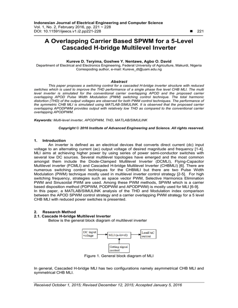
Below is the general block diagram of multilevel inverter
Figure 1. General block diagram of MLI
In general, Cascaded H-bridge MLI has two configurations namely asymmetrical CHB MLI and
symmetrical CHB MLI.
Received October 1, 2015; Revised December 12, 2015; Accepted January 5, 2016
222
ISSN: 2502-4752
2.1.1. Asymmetrical CHB MLI
Asymmetrical cascaded H-bridge multilevel inverter. These are CHB MLI in which at
least one of the dc supply source presents different amplitude, that is H-bridge cells are not fed
by equal voltage and the arm cells have different effect on the output voltage steps.
Asymmetrical MLI is illustrated with five levels in the figure below.
Figure 3. 7-level asymmetrical CHB MLI
2.1.2. Symmetrical CHB MLI
Symmetrical cascaded H-bridge multilevel inverter are the one in which the amplitude of
the entire dc supply source to each H-bridge cells is equal [4].
Figure 2. 5-level symmetrical CHB MLI
For example, each level can generate five different voltage outputs ±2Vdc, ±1Vdc, and
0Vdc by switching the different switches on and off. The output voltage of a multilevel inverter is
the sum of all the individual inverter outputs.
⋯
⁄
(1)
Where: Van = 1-Ø voltage output, Va1…an= Output Voltage of individual modules, x= number of
levels.
The Fourier transform for the stepped waveform is expressed as:
V(ωt)=
π
Σ[cos(nθ1)+cos(nθ2)+...+cos(nθs)]sin(nωt)/n
Where n=1, 3, 5, 7, .,.
IJEECS Vol. 1, No. 2, February 2016 : 221 – 228
(2)
ISSN: 2502-4752
IJEECS
223
Each H-bridge unit generates a staircase waveform by phase-shifting its positive and
negative phase switching timings. Further, each switching MOSFET always conducts for 180˚
(or half cycle) regardless of the pulse width of the quasi-square wave so that this switching
method results in equalizing the current stress in each active device. Cascaded H-bridge
topology is chosen for this paper.
2.2. Advantages of Cascaded H-bridge MLI
The advantages of CHB MLI configuration are [3]:
a) Staircase wave form quality which reduces electromagnetic compactibilty.
b) Modularity of control can be achieved.
c) Requires less number of components to achieve the same number of output
voltage levels.
d) Draws input current with low distortion.
2.3. Disadvantages of Cascaded H-bridge MLI
The disadvantages of CHB MLI configuration are [3]:
a) Communication between the full-bridges is required to achieve the synchronization
of reference and the carrier waveforms.
b) Needs separate dc sources for real power conversions, and thus its applications
are somewhat limited.
2.4. Types of Carrier based SPWM Techniques
There are different forms of modulation techniques for MLI. Generally, in the pulse width
modulation technique, two signals are used, one is reference signal and the other is carrier
signal [8].
This paper applied carrier based PWM techniques to the CHB-MLI by using multiple
carrier waveforms and a sinusoidal reference wave form [10-12]. The number of carrier
waveforms required to produce Y level output is (x-1), where x is the number of carrier
waveforms [8].
The sinusoidal reference waveform has peak amplitude Am and a modulating frequency
fm. The triangular carrier waveforms have a peak amplitude Ac and frequency fc. The sinusoidal
reference signal is continuously compared with all the triangular carrier waveforms. Whenever
the sinusoidal reference signal/waveform is greater than the carrier signal, a modulated pulse
width is generated. The modulation frequency ratio mf is given as:
.
(3)
The following are Carrier based Overlapping SPWM strategies:
1) Carrier Overlapping Phase Disposition PWM strategy (CO-PD PWM):
If all carriers selected have the same phase, the method is phase disposition method. It
is generally accepted that this method gives rise to the lowest harmonic distortion in higher
modulation indices. Figure 4 shows the arrangement phase disposition PWM method.
Figure 4. Arrangement of carrier overlapping phase disposition PWM method
A Overlapping Carrier Based SPWM for a 5-Level Cascaded H-bridge… (Kureve D. Teryima)
224
ISSN: 2502-4752
Figure 4 depicts the Carrier overlapping PD PWM technique (CO-PD PWM), where the
carriers with the same frequency fc and peak amplitude Ac are arranged such that they overlap
each other [5].
2) Carrier Overlapping Phase Opposition Disposition PWM strategy (CO-POD PWM):
The carrier waves in the positive plane are 180o out of phase with those in the negative plane.
There is no harmonic at the carrier frequency and its multiples and the dispersion of harmonic
occurs around them.
Figure 5. Arrangement of carrier overlapping POD PWM method
3) Carrier Overlapping Alternate Phase Opposition Disposition PWM strategy (COAPOD PWM):
Each carrier in this method is phase shifted by 1800 from its adjacent carrier. It is similar
to phase opposition disposition. Figure 6 shows the overlapping carrier APOD PWM strategy.
Figure 6. The arrangement of carrier overlapping APOD PWM method
Amplitude modulation index for Carrier Overlapping PD PWM, POD PWM, and APOD
PWM is:
(4)
2.5. Simulation Model
The cascaded 5-level single phase CHB MLI used for this implementation has two dc
sources and six switches as shown in Figure 7.
IJEECS Vol. 1, No. 2, February 2016 : 221 – 228
ISSN: 2502-4752
IJEECS
225
Discrete,
Ts = 5e-005 s.
m
S
S
DC Voltage 1
[notB 1]
boolean
g
S
m
D
From 3
boolean
Series RLC Branch
Mosfet 4
double
+
v
-
m
Voltage Measurement
Scope 4
S
D
Mosfet 1
g
From 2
g
g
D
Mosfet 3
m
Mosfet
D
From 1
From
[notB ]
boolean
[A1]
boolean
[A]
DC Voltage 2
m
S
m
Mosfet 5
S
Mosfet 2
boolean
g
[C1]
From 5
D
g
boolean
D
[C]
From 4
Figure 7. 5-level single phase CHB-MLI
The main advantage of this type of arrangement is its simplicity and improvement of the
output voltage resolution with reduced number of components [11].
2.5.1. Operation of Cascaded H-bridge of Five-level MLI Topology
In an individual H-bridge, the output voltage is positive voltage (+Vdc), zero voltage
(0Vdc) and negative voltage (-Vdc). Hence the desired output voltage levels for Five-level CHB
MLI are ±2V, ±1V, and 0V.
The switching states for the voltage levels are presented as shown in the table below:
Table 1. Switching states of modified 5-level CHB MLI
Voltage
levels
Switching sequences
S1
0
0
1
1
1
S2
1
1
1
0
0
S3
0
1
1
0
1
S4
1
1
0
0
0
S5
0
0
0
1
1
S6
1
0
0
1
0
+2Vdc
+1Vdc
0Vdc
-1Vdc
-2Vdc
The above circuit diagram in Figure 7 and its switching state in Table 1 have been
modified to avoid switching loss and unnecessary cost. This CHB MLI with six switches and two
batteries will improve output waveform and reduce total harmonic distortion. One of the
distinguishing features of the above circuit is that it can be used as seven level and five level
CHB MLI respectively, by making the two dc input voltages to be different (asymmetric) and
make the two dc input voltage equal (symmetric).
2.6. Proposed Overlapping APODPWM Technique
The new switching technique deployed for this paper is the carrier based overlapping
APOD PWM with non-zero overlap. The strategy used in this form of technique is a modified
overlapping APODPWM technique already known. It involves placing the triangular signals in
overlapping mode without crossing the zero time axis. They are aligned both in the positive and
negative planes respectively. This is illustrated as shown in the Figure below:
A Overlapping Carrier Based SPWM for a 5-Level Cascaded H-bridge… (Kureve D. Teryima)
226
ISSN: 2502-4752
Figure 8. The arrangement of the proposed carrier overlapping APOD PWM
This form of switching is carried out at a carrier frequency of 5 kHz and a fundamental
frequency of 50 Hz.
3.
Results and Analysis
Simulation of the suggested modulation techniques for comparison for a CHB MLI with
reduced switches is carried out using MATLAB/SIMULINK and the following parameters were
used: Vdc =100V, fc= 5 kHz and fm= 50 Hz, Ma=1.0. The Simulated control techniques, Output
Voltage waveform and FFT analysis of the 5-level CHB-MLI using both the CO-APOD and the
proposed CO-APOD PWM are presented.
2
1.5
1
0.5
0
-0.5
-1
-1.5
-2
0
0.002
0.004
0.006
0.008
0.01
0.012
0.014
0.016
0.018
0.02
Figure 10. Reference and carrier frequency signal of CO-APOD
3
2
1
0
-1
-2
-3
0
0.002
0.004
0.006
0.008
0.01
0.012
0.014
0.016
0.018
0.02
Figure 11. Reference and carrier frequency signal of proposed CO-APOD
IJEECS Vol. 1, No. 2, February 2016 : 221 – 228
ISSN: 2502-4752
IJEECS
227
The reference signal being super imposed on the six carrier signals are generated via
logic combination in SIMULINK and are used for switching the gates of the power MOSFETS. A
point to note is that for the proposed CO-APOD, there is no overlap across the zero time axes.
The uniqueness of the proposed CO-APOD modulation scheme adopted herein is that it
distributes the load evenly across the switching components thereby reduce switching losses.
60
40
20
0
-20
-40
-60
0
0.01
0.02
0.03
0.04
0.05
0.06
0.07
0.08
0.09
0.1
Figure 12. Output waveform of 5-level single phase CHB MLI in SIMULINK for CO-APOD
200
150
100
50
0
-50
-100
-150
-200
0
0.01
0.02
0.03
0.04
0.05
0.06
0.07
0.08
0.09
0.1
Figure 13.Output waveform of 5-levels single phase CHB MLI in SIMULINK for proposed
CO-APOD
Figure 14. FFT analysis of THD for 5-level
CHB MLI using CO-APOD
Figure 15. FFT analysis of THD for 5-level
CHB MLI using proposed CO-APOD
A Overlapping Carrier Based SPWM for a 5-Level Cascaded H-bridge… (Kureve D. Teryima)
228
ISSN: 2502-4752
The above graph represents the THD of the 5-level single phase CHB MLI for the
different modulation techniques.
In the CO-APOD, the even order harmonics are eliminated as shown in Figure 14 but in
the proposed CO-APOD FFT analysis as shown in Figure 15, the even order harmonics are
completely eliminated.
4.
Conclusion
This paper suggests a novel PWM technique using overlapping APOD PWM for
switching pulses of a 5 level Cascaded Multilevel Inverter with reduced number of H-bridges
while producing desired multilevel voltage output. Simulation using MATLAB/SIMULINK
software was performed to show the suggested technique for CO-APOD PWM performed better
with a THD of 34.44 % as compared to the conventional CO-APOD PWM with a THD of 39.76%
References
[1] FZ Peng, JS Lai. Multilevel converters, A new breed of power Electronics converters. IEEE Trans
Industries Application. 2003: 1098-1107.
[2] J Rodriguez, JS Lai, FZ Peng. Multilevel Inverter; A survey topology control and application. IEEE
Trans Industrial Electronics. 2003: 724-738.
[3] Kumar Jagdish. THD Analysis for different levels of cascade multilevel inverter for industrials
applications. IJETAE. 2012: 20-30.
[4] M Kavitha, A Arunkumar, N Gokulnath, S Arun. New cascaded H-bridge multilevel inverter topology
with reduced number of switches and sources. JEEE. 2012: 26-36.
[5] G Prem Sunder, B Shanthi, ALamehi Nachiappan, SP Natrajan. Performance Analysis of modified
CHB MLI using various carrier modulation schemes. IJESA. 2013; 3(5): 310-316.
[6] E Sambath, SP Natarajan, CR Balamurugan. Performance Evaluation of Multi Carrier Based PWM
Techniques for Single Phase Five Level H-Bridge Type FCMLI. IOSR Journal of Engineering. 2012;
2(7): 82-90.
[7] Vinayaka BC, S Nagendra Prasad. Modeling and design of 5-level CHB MLI with dc/dc boost
converter. International journal of Engineering research and Application. 2014.
[8] R Rajesh, M Balasubtamani, J Gowrishankar. Newly constructed single phase multilevel inverter for
distributed energy resources. IJET. 2013: 1445-1452.
[9] Upvan Tamrakar, CS Sharma, Sudhir Phulambrikar. Analysis and simulation of single phase and
three phase seven level inverter. International Journal for Scientific Research and Development. 2014;
2(7).
[10] Ebrahim Babaci. A cascaded multilevel converter topology with reduced number of switches. IEEE
Trans on Power Electronics. 2008l; 23(6).
[11] C Kannan, CK Kishore. A Comparision of Three Phase 27 Level Inverter Scheme under No Load and
Multiple Load Conditions. Bulletin of Electrical Engineering and Informatics. 2014; 3(4): 245-250.
[12] Suroso, Agung Mubyarto, Toshihiko Noguchi, A Different Single-Phase Hybrid Five-Level Voltage
Source Inverter Using DC-Voltage Modules. TELKOMNIKA. 2014; 12(3): 557-562.
IJEECS Vol. 1, No. 2, February 2016 : 221 – 228
