BJT Transistor Modeling
advertisement

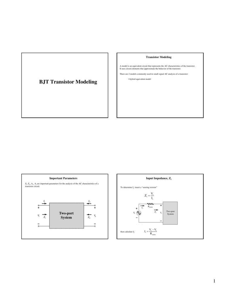
Transistor Modeling A model is an equivalent circuit that represents the AC characteristics of the transistor. It uses circuit elements that approximate the behavior of the transistor. There are 2 models commonly used in small signal AC analysis of a transistor: BJT Transistor Modeling • hybrid equivalent model Important Parameters Zi, Zo, Av, Ai are important parameters for the analysis of the AC characteristics of a transistor circuit. Input Impedance, Zi To determine Ii: insert a “sensing resistor” Zi = then calculate Ii: Ii = Vi Ii Vs − Vi R sense 1 Output Impedance, Zo Voltage Gain, Av Av = To determine Io: insert a “sensing resistor” Zo = then calculate Io: Io = Vo Io V − Vo R sense For an amplifier with no load: Io Ii Vo Vi R L = ∞ Ω (opencircuit) Note: the no-load voltage gain (AVNL) is always greater than the loaded voltage gain (AV). Current Gain, Ai Ai = A VNL = Vo Vi Phase Relationship The phase relationship between input and output depends on the amplifier configuration circuit. Common – Emitter : 180 degrees Common - Base : 0 degrees Common – Collector: 0 degrees The current gain (Ai) also be calculated using the voltage gain (Av): A i = −A v Zi RL 2 Hybrid Equivalent Model General h-Parameters for any Transistor Configuration The hybrid parameters: hie, hre, hfe, hoe are developed and used to model the transistor. These parameters can be found in a specification sheet for a transistor. • hi = input resistance • hr = reverse transfer voltage ratio (Vi/Vo) • hf = forward transfer current ratio (Io/Ii) • ho = output conductance hi = input resistance hr = reverse transfer voltage ratio (Vi/Vo) hf = forward transfer current ratio (Io/Ii) ho = output conductance Simplified General h-Parameter Model Common-Emitter h-Parameters The above model can be simplified based on these approximations: hr ≅ 0 therefore hrVo = 0 and ho ≅ ∞ h ie = 25mV h fe 25mV ≅ I BQ I EQ h fe = β ac 3 Common-Base h-Parameters BJT Small-Signal Analysis h ib = 25mV I EQ h fb = −α ac ≅ −1 Common-Emitter (CE) Fixed-Bias Configuration Removing DC effects of VCC and Capacitors ⇒ Hybrid Equivalent Circuit The input (Vi) is applied to the base and the output (Vo) is from the collector. The Common-Emitter is characterized as having high input impedance and low output impedance with a high voltage and current gain. 4 Hybrid Equivalent Circuit Impedance Calculations Input Impedance: Determine hfe, hie, and hoe: hfe and hoe: look in the specification sheet for the transistor or test the transistor using a curve tracer. hie: calculate hie using DC analysis: h ie = 25mV 25mV ≅ h fe I BQ I EQ Gain Calculations Voltage Gain (Av): Current Gain (Ai): Av = Ai = vo h (R || 1/h oe ) = − fe C vi h ie Av = − h fe R C h ie Zi = R B || h ie Zi ≅ h ie Output Impedance: 1 Zo = R C || h oe R B ≥10h ie Zo ≅ R C 1/h oe ≥10 R C Phase Relationship 1/h oe ≥ 10R C io h fe R B (1/h oe ) = i i (1/h oe + R C )(R B + h ie ) A i ≅ h fe Current Gain from Voltage Gain: A i = −A v Zi RC 1/h oe ≥ 10R C , R B ≥ 10 h ie The phase relationship between input and output is 180 degrees. The negative sign used in the voltage gain formulas indicates the inversion. 5 CE – Voltage-Divider Bias Configuration Impedance Calculations ⇓ Input Impedance: Zi = R ′ || h ie Output Impedance: Z o = R C || You still need to determine hfe, hie, and hoe. Gain Calculations 1 h oe R ′ = R 1 || R 2 = Zo ≅ R C R 1R 2 R1 + R 2 1/h oe ≥ 10R C Phase Relationship A CE amplifier configuration will always have a phase relationship between input and output is 180 degrees. This is independent of the DC bias. Voltage Gain (Av): Av = Current Gain (Ai): A i = vo R || 1/h oe = − h fe C vi h ie h fe R C h ie 1/h oe ≥ 10R C h fe R ′ R ′ + h ie 1/h oe ≥ 10R C Av ≅ − io h fe R ′ (1/h oe ) = i i (1/h oe + R C )(R ′ + h ie ) Ai ≅ A i ≅ h fe 1/h Current Gain from Voltage Gain: A i = −A v oe ≥ 10R C , R ′≥ 10h ie Zi RC 6 CE Emitter-Bias Configuration Impedance Calculations Unbypassed RE Input Impedance: Zi = R B || Z b Z b = h ie + ( h fe + 1)R E Z b ≅ h fe R E (h Again you need to determine hfe, hie. Output Impedance: Gain Calculations fe +1)R E >> h ie , h fe >> 1 Zo = R C Phase Relationship A CE amplifier configuration will always have a phase relationship between input and output is 180 degrees. This is independent of the DC bias. Voltage Gain (Av): Current Gain (Ai): Av = Ai = vo h R = − fe C vi Zb Av ≅ − RC RE Z b ≅ h fe R E io h R = fe B ii R B + Zb Current Gain from Voltage Gain: A i = −A v Zi RC 7 Emitter-Follower Configuration Hybrid Equivalent Model You may recognize this as the Common-Collector configuration. Indeed they are the same circuit. You still need to determine hfe and hie. Note the input is on the base and the output is from the emitter. Impedance Calculations Input Impedance: Zi = R B || Z b Impedance Calculations (cont’d) Z b = h ie + ( h fe + 1)R E Z b ≅ h fe R E (h fe +1)R E >> h ie , h fe >> 1 Output Impedance: Z o = R E || Zo ≅ h ie h fe h ie h fe + 1 (h fe +1)R E >> h ie , h fe >> 1 8 Phase Relationship Gain Calculations A CC amplifier or Emitter Follower configuration has no phase shift between input and output. Voltage Gain (Av): Current Gain (Ai): Av = Ai ≅ vo RE = v i R E + h ie /( h fe + 1) Av ≅ 1 (h fe +1)R E >> h ie io h R − fe B ii R B + Zb Current Gain from Voltage Gain: A i = −A v Zi RE Common-Base (CB) Configuration Hybrid Equivalent Model You will need to determine hfb and hib. The input (Vi) is applied to the emitter and the output (Vo) is from the collector. The Common-Base is characterized as having low input impedance and high output impedance with a current gain less than 1 and a very high voltage gain. h ib = h ie 25mV = h fe + 1 I EQ h fb = − α ac ≅ −1 9 Gain Calculations Impedance Calculations Voltage Gain (Av): Input Impedance: Output Impedance: Av = v o h fb R C R C = ≅ vi h ib h ib Zi = R E || h ib Zo = R C Phase Relationship Current Gain (Ai): Ai = io = h fb ≅ −1 ii CE Collector Feedback Configuration A CB amplifier configuration has no phase shift between input and output. This is a variation of the CE Fixed-Bias configuration. 10 Impedance Calculations Hybrid Equivalent Model Input Impedance: You will need to determine hfe and hie. Output Impedance: Zi = h ie 1 + h fe RC RF Zo ≅ R C || R F Example Gain Calculations Voltage Gain (Av): Av = Current Gain (Ai): Ai = hfe = hFE = 200 ICO = 0 A VBE = 0.7 V VCEsat = 0 V Vo h R = − fe C Vi h ie Io h fe R F = Ii R F + h fe R C Ai = Io R F ≅ Ii R C According to the figure above – – – Perform DC analysis and find the Q-point. Evaluate the voltage gain Avs and the current gain Ai. Sketch vo on the AC+DC load line graph when • • vs = 100 sin(wt) mV. vs = 900 sin(wt) mV. ICQ = 0.39 mA VCBQ = 6.8 V ⇒ 11


