Quantum Facts
“Improving the Quality of Life through the Power in Light”
Series: QF2-01
LED THEORY A ND APPLICATION NOTES
…GENERAL…
A Light-Emitting-Diode (LED) is a P-N junction
device (diode) that gives off light radiation
when biased in the forward direction. LED
chip materials are combinations of elements
from the III and V columns of the periodic
chart.
The light emitting phenomenon makes use of
the recombination within the P-N junction
instead of thermal radiation, therefore, LED’s
are free of waste and wear and can be
expected to have a long life time. By
controlling the forward current, the radiant flux
of the LED can be easily controlled. The
response time of an LED is very high (a few
hundred nanoseconds) and can be pulsed at
greater forward currents, to obtain high
intensity radiant peaks. The resin packaging
of LED’s allow for superb mechanical integrity
and can withstand dropping, vibration and
shock. These semiconductor devices can be
mounted in any position.
…THEORY…
Just as it takes energy to generate a hole-electron pair, energy is released when an electron recombines
with a hole. If a forward current is passed through a semiconductor diode, electrons and holes are
injected into the P and N region respectively. Depending on the magnitude of the current, a
recombination of charge carriers (electron and holes) takes place when an electron falls from the
conduction into the valence band. In silicon and germanium when this recombination takes place, the
surplus energy goes into the crystal as heat. In other semiconductors, such as gallium arsenide, the
released energy appears in the form of electromagnetic radiation, ranging from visible to infrared. The
wavelength of this radiation is dependent on energy required to cause electrons to jump from the
conduction band to the valence band.
A portion of the light generated within the LED is unable to emerge due to internal absorption, fresnel
losses and internal reflection. Internal absorption occurs as a photon is traveling from the junction region
through the chip. Limiting the range of this travel will reduce the internal absorption, thus smaller LED
sizes will manifest increased conversion efficiencies. Fresnel losses and internal reflection are minimized
by covering the LED chip with an optical coating material whose index of refraction will bridge the indices
of refraction between the chip and air.
Light is concentrated near the junction because most of the carriers are to be found within a diffusion
length of the junction. Since this junction extends to and is exposed on all four sides of the die, a
considerable amount of energy is emitted from the sides as well as the top surface. Typically, the LED
chip is mounted in a conical cavity to reflect the side emitting energy forward.
ELECTRICAL CONSIDERATIONS
BASIC DC CIRCUIT
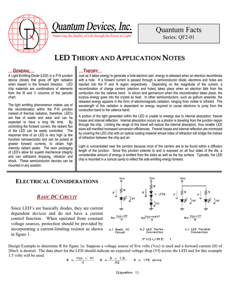
Since LED’s are basically diodes, they are current
dependent devices and do not have a current
control function. When operated from constant
voltage sources, protection should be provided by
incorporating a current-limiting resistor as shown
in figure 1.
Design Example to determine R for figure 1a: Suppose a voltage source of five volts (Vcc) is used and a forward current (If) of
20mA is desired. The data sheet for the LED should indicate an expected voltage drop (Vf) across the LED and for this example
1.5 volts will be used.
Pg. 1
LED INTERFACE CIRCUITRY
CONSTANT CURRENT REGULATORS
This type of DC drive will regulate the current
flow through the LED. There are numerous
constant current regulator circuits and the circuit
shown in figure 2 can be used for a single LED as
shown or a number of devices in series.
BASIC AC CIRCUIT
Since LED’s should be operated in the forward direction, reverse
voltage protection is required to assure the reverse voltage (Vr)
maximum is not exceeded. Figure 3a illustrates the placement of
back-to-back silicon diode across the LED, the silicon diode will
clamp the voltage across the LED to approximately .6 volts.
Figure 3b shows a different approach that uses two (2) LED’s in
parallel which alternately light relative to the device under a
forward bias condition.
BASIC TRANSISTOR DRIVE CIRCUIT
Figure 4a shows a transistor
drive circuit that lights the
LED when the transistor is
conducting into saturation
Figure 4b shows a transistor drive
circuit that lights the LED when the
transistor is not conducting or is
considered to be open. Equation 1
should be used to determine the
value of R. Both of the transistor
drive circuits shown in figure 4 can
be configured to drive multiple
LED’s in series
The value R is calculated as shown
below:
PULSED OPERATION
Pulsed operation of LED’s can typically be achieved by the transistor drive circuits shown in figure 4. Significantly higher peak
LED light output can be realized from large drive current pulses at a low duty cycle. The maximum tolerable limits should not
exceed the LED junction temperature above that obtained by operating the lamp at the maximum DC current
Pg. 2
LED PACK AGING
LED DIE
The actual size of an LED chip die is typically a cube that is .4mm (.016”) on
all three sides and is simply illustrated in figure 5. The anode and cathode
contacts are opposite each other on the top and bottom of the die. Depending
on the processes utilized, and anode and cathode contacts can be on either side
of the die. The contact to the bottom side is accomplished by using conductive
adhesive to attach the die to a conductive substrate. Usually a wire (1 mil in
diameter) is fastened to the bond pad on top and is further attached to an
external contact or substrate. The bond wire attachment is accomplished using
thermal compression or ultrasonic bonding processes.
COMMON PACKAGING
CUSTOM PACKAGING
LED’s are commonly packaged in a resin cast or molded
plastic enclosure as shown in figure 6. The LED die is
attached to the reflector side of a lead frame and a bond wire is
attached between the top of the die and the opposite lead
frame contact. The lead frame containing the assembled LED
proceeds to the final casting or molding process for
encapsulation. Typically, the flat side of the package
designates the cathode lead. The casting process will form a
lens at the tip of the component to maximize light in the
forward direction. The shape of the lens and the placement of
the lead frame is altered to conform to the desired beam
pattern or viewing angle.
LED die can be assembled
onto many different substrates
to include; ceramic, metal,
printed circuit boards and flex
circuits,
and
can
be
encapsulated to protect the die
and bond wire connection.
Many different reflector, lens,
and optical configurations can
be achieved. Please contact
the factory to discuss your
application with an engineer.
RADIO METRIC MEASUREMENTS
RADIANT FLUX
Radiant Flux is the time rate of flow of radiant energy measured in watts and can be
specified as power output. The radiant flux of an LED is measured with an
integrating sphere and radiometer combination.
This type of measurement offers a high degree of reproducibility in that nearly all of
the power emitted by the integrating spheres consist of two hemispheres that are
mated together to form a spherical cavity. The sphere is constructed so that the inner
surface consists of a highly reflective diffuse material. Radiation introduced into the
sphere and incident upon the surface of the sphere wall is reflected in random
directions. The interior of the sphere is characterized by a spatially integrated
radiation distribution which is very uniform and this level is proportional to the total
amount of radiation introduced into the sphere. A photodetector mounted at a port on
the sphere wall to the external radiometer senses the flux density. The measurement
of total radiometric flux does not further define spatial distribution or energy
contained within angular beam pattern.
RADIANT INTENSITY
Radiant Intensity is the radiant energy emitted within a time period per unit solid angle, usually measured in watts per steradian. A surface
area of a steradian extending from the center of a sphere is equivalent to the square of the radius. There are 4 steradians in a sphere and in a
pure cone, a steradian subtends a solid angle of about 66 degrees.
In laymen terms, the measurement procedure is similar to measuring radiant flux. The difference is the photodiode is mounted at a
specified distance from, and on the mechanical axis of the LED. An aperture is placed over the photodiode whose opening is the square of
the distance from the LED so that only the detector is 10cm and the active area of the detector is one square cm. This results in a solid
angle of .01 steradians (fig. 8). The radiant intensity is obtained by using this measured detector value for calculating the radiant intensity
for a solid angle of one steradian, i.e. the resultant power measurement is factored by 100 to convert the answer to watts per steradian.
Pg. 3
cont. from page 3
This type of measurement results in the on-axis
power intensity of the LED over a particular
beam angle which is typically a steradian. The
radiant intensity value may quantify the
requirements for a particular design. The
repeatability
of
the
radiant
intensity
measurement is demanding, due to the difficulty
in establishing the mechanical axis.
SOLDERING INSTRUCTIONS
Precaution against overheating must be exercised to prevent damage to the LED. It is recommended the applied heat should be as short
as possible and any heat generated be quickly conducted away. Generally a soldering temperature of less than 260 deg. C, at a distance
of 2mm from the case, should have a soldering dwell time of less than 3 seconds. Normal flux cleaning processes should be acceptable,
however experimentation is recommended.
F OR MORE INFORMATION CONTACT…
Quantum Devices, Inc.
112 Orbison St.
P.O. Box 100
Barneveld, WI 53507
Tel: (608)924-3000
Fax: (608)924-3007
URL: www.quantumdev.com
E-mail: qdisales@quantumdev.com
© Quantum Devices, Inc. 1998. All rights reserved
Pg. 4
