Sept. 1995
Edition 3.0b
DATA SHEET
MB510
2.7GHz TWO MODULUS PRESCALER
2.7GHz TWO MODULUS PRESCALER
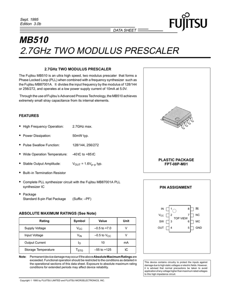
The Fujitsu MB510 is an ultra high speed, two modulus prescaler that forms a
Phase Locked Loop (PLL) when combined with a frequency synthesizer such as
the Fujitsu MB87001A. It divides the input frequency by the modulus of 128/144
or 256/272, and operates at a low power supply current of 10mA at 5.0V.
Through the use of Fujitsu’s Advanced Process Technology, the MB510 achieves
extremely small stray capacitance from its internal elements.
FEATURES
High Frequency Operation:
2.7GHz max.
Power Dissipation:
50mW typ.
Pulse Swallow Function:
128/144, 256/272
Wide Operation Temperature:
-40°C to +85°C
Stable Output Amplitude:
VOUT = 1.6Vp–p typ.
Built–in Termination Resistor
PLASTIC PACKAGE
FPT-08P-M01
Complete PLL synthesizer circuit with the Fujitsu MB87001A PLL
synthesizer IC
Package
Standard 8-pin Flat Package
PIN ASSIGNMENT
(Suffix: –PF)
ABSOLUTE MAXIMUM RATINGS (See Note)
Rating
IN
1
VCC
2
8
IN
7
NC
TOP VIEW
Symbol
Value
Unit
SW
3
6
MC
Supply Voltage
VCC
–0.5 to +7.0
V
OUT
4
5
GND
Input Voltage
VIN
–0.5 to VCC
V
Output Current
IO
10
mA
TSTG
–55 to +125
°C
Storage Temperature
Note:
Permanent device damage may occur if the above Absolute Maximum Ratings are
exceeded. Functional operation should be restricted to the conditions as detailed in
the operational sections of this data sheet. Exposure to absolute maximum rating
conditions for extended periods may affect device reliability.
Copyright 1995 by FUJITSU LIMITED and FUJITSU MICROELECTRONICS, INC.
This device contains circuitry to protect the inputs against
damage due to high static voltages or electric fields. However,
it is advised that normal precautions be taken to avoid
application of any voltage higher than maximum rated voltages
to this high impedance circuit.
MB510
INPUT BUFFER
IN
IN
D Q
D Q
D Q
C
C Q
CM Q
MC
D Q
D Q
D Q
D Q
C Q
C Q
C Q
C Q
D Q
D Q
C Q
SW Q
SW
SW
MC
Divide Ratio
H
H
1/128
H
L
1/144
L
H
1/256
L
L
1/272
Note:
SW: H = VCC, L = open
MC: H = 2.0V to VCC, L = GND to 0.8V
Figure 1. MB510 Block Diagram
PIN DESCRIPTION
2
Pin Number
Symbol
Function
1
IN
2
VCC
DC Supply Voltage
3
SW
Divide Ratio Control Input (See Divide Ratio Table)
4
OUT
Output
5
GND
Ground
6
MC
Modulus Control Input (See Divide Ratio Table)
7
NC
Non Connection
8
IN
Complementary Input
Input
OUTPUT
BUFFER
OUT
MB510
RECOMMENDED OPERATING CONDITIONS
Value
Parameter
Symbol
Supply Voltage
VCC
Output Current
IO
Ambient Temperature
TA
Load Capacitance
CL
Unit
Min.
Typ.
Max.
4.5
5.0
5.5
1.2
–40
V
mA
+85
°C
8
pF
ELECTRICAL CHARACTERISTICS
(Recommended Operating Conditions unless otherwise noted)
Value
Parameter
Symbol
Condition
Unit
Min.
Typ.
Max.
10.0
15.0
Supply Curent
ICC
Output Amplitude
VO
Built-in a termination
resistor.
Load capacitance = 8pF
1.0
Input Frequency
fIN
With input coupling
capacitor 1000pF
10
2700
10
PIN
fIN = 10 to 2200MHz
–10
Input Signal Amplitude
fIN = 2200 to 2700MHz
–4
10
High Level Input Voltage for MC
Input
VIHM
Low Level Input Voltage for MC
Input
VILM
High Level Input Voltage for SW
Input
VIHS*
Low Level Input Voltage for SW
Input
VILS
High Level Input Current for MC
Input
IIHM
VIH = 2.0V
Low Level Input Current for MC
Input
IILM
VIL = 0.8V
Modulus Set-up Time MC to OUT
tSET
Note:
1.6
mA
Vp–p
MHz
dBm
2.0
VCC –0.1
V
VCC
0.8
V
VCC +0.1
V
Open
V
0.4
–0.2
mA
mA
16
26
ns
*Design Guarantee
3
MB510
VCC = +5.0V + 10%
C3
Sampling scope input point
for input waveform
VCC
SW
C1
OUT
IN
P.G.
50Ω
Sampling scope prober point
for output waveform
IN
CL
C2
MC GND
MC Input
C1 : 1000pF
C2 : 1000pF
C3 : 0.1µF
CL : 8pF (including scope and jig capacitance)
MINIMUM INPUT SIGNAL AMPLITUDE (mVp–p)
Figure 2. Test Circuit
VCC = 5.0V
TA = 25°C
800
600
500
400
300
200
100
10
20
50 100 200
500 1000 2000
INPUT FREQUENCY (MHz)
Figure 3. Input Signal Amplitude vs. Input Frequency
4
MB510
TIMING CHART (2 MODULUS)
Example: Divide ratio = 128/144
128
144
IN
64
64
64
80
OUT
64 64 64 64
64 64 80 64 80 64 80
MC
tSET
tSET
Note: When divide of 144 is selected, positive pulse is applied by 16 to 80.
The typical set up time is 16 ns from the MC signal input to the timing of change of prescaler divide ratio.
C1
VSX (Max. 8V)
VCC
VCC
VCC
10KΩ
C2
X1
12KΩ
16 15 14 13 12 11 10 9
VCO
MB 87001A
0.047µF
1
2 3 4
5 6
OUTPUT
12KΩ
VCC
7 8
100KΩ
10KΩ
33KΩ
47K
47K
47K
Clock
Data
LE
1000pF
1000pF
8
7
6
5
MB 510
VCC
1000pF
1
2
3
4
1000pF
2.2KΩ
X1
VCC
VSX
C1, C2
:
:
:
:
12.8MHz X’tal
5V + 10%
8V max.
depends on crystal oscillator
Lock
Det.
10KΩ
Figure 4. Typical Application Example
5
MB510
PACKAGE DIMENSIONS
(Suffix: –PF)
8-LEAD PLASTIC FLAT PACKAGE
(CASE No: FPT-08P-M01)
.010
.250 – .008
0.25
6.35 – 0.20
.089(2.25) MAX
(SEATED HEIGHT)
.002(0.05) MIN
(STAND OFF)
.307+.016
(7.80+0.40)
INDEX
.016
.268 – .008
.209+.012
(5.30+0.30)
0.40
6.80 – 0.20
.020+.008
(0.50+0.20)
.050(1.27)
.018+.004
(0.45+0.10)
TYP
∅ .005(0.13)
M
.002
.006 – .001
0.05
0.15 – 0.02
.150(3.81)
Details of “A” part
REF
“A”
.004(0.10)
1988 FUJITSU LIMITED F08002S-3C
All Rights Reserved.
Circuit diagrams utilizing Fujitsu products are included as a means of illustrating typical
semiconductor applications. Complete information sufficient for construction purposes is
not necessarily given.
The information contained in this document has been carefully checked and is believed to
be reliable. However, Fujitsu assumes no responsibility for inaccuracies.
The information contained in this document does not convey any license under the copyrights, patent rights or trademarks claimed and owned by Fujitsu.
Fujitsu reserves the right to change products or specifications without notice.
No part of this publication may be copied or reproduced in any form or by any means, or
transferred to any third party without prior written consent of Fujitsu.
6
.008(0.20)
.020(0.50)
.007(0.18)
MAX
.027(0.68)
MAX
DImensions in
inches (millimeters)


