as a PDF
advertisement

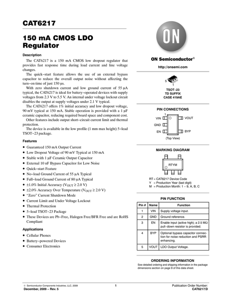
CAT6217 150 mA CMOS LDO Regulator Description The CAT6217 is a 150 mA CMOS low dropout regulator that provides fast response time during load current and line voltage changes. The quick−start feature allows the use of an external bypass capacitor to reduce the overall output noise without affecting the turn−on time of just 150 ms. With zero shutdown current and low ground current of 55 mA typical, the CAT6217 is ideal for battery−operated devices with supply voltages from 2.3 V to 5.5 V. An internal under voltage lockout circuit disables the output at supply voltages under 2.1 V typical. The CAT6217 offers 1% initial accuracy and low dropout voltage, 90 mV typical at 150 mA. Stable operation is provided with a 1 mF ceramic capacitor, reducing required board space and component cost. Other features include output short−circuit current limit and thermal protection. The device is available in the low profile (1 mm max height) 5−lead TSOT−23 package. http://onsemi.com 5 1 TSOT−23 TD SUFFIX CASE 419AE PIN CONNECTIONS 1 GND BYP EN (Top View) Features • • • • • • • • • • • • • • VOUT VIN Guaranteed 150 mA Output Current Low Dropout Voltage of 90 mV Typical at 150 mA Stable with 1 mF Ceramic Output Capacitor External 10 nF Bypass Capacitor for Low Noise Quick−start Feature No−load Ground Current of 55 mA Typical Full−load Ground Current of 80 mA Typical ±1.0% Initial Accuracy (VOUT ≥ 2.0 V) ±2.0% Accuracy Over Temperature (VOUT ≥ 2.0 V) “Zero” Current Shutdown Mode Current Limit and Under Voltage Lockout Thermal Protection 5−lead TSOT−23 Package These Devices are Pb−Free, Halogen Free/BFR Free and are RoHS Compliant Applications • Cellular Phones • Battery−powered Devices • Consumer Electronics MARKING DIAGRAM RTYM RT = CAT6217 Device Code Y = Production Year (last digit) M = Production Month: 1 − 9, A, B, C PIN FUNCTION Pin # Name 1 VIN Supply voltage input. 2 GND Ground reference. 3 EN Enable input (active high); a 2.5 MW pull−down resistor is provided. 4 BYP Optional bypass capacitor connection for noise reduction and PSRR enhancing. 5 Function VOUT LDO Output Voltage. ORDERING INFORMATION See detailed ordering and shipping information in the package dimensions section on page 9 of this data sheet. © Semiconductor Components Industries, LLC, 2009 December, 2009 − Rev. 5 1 Publication Order Number: CAT6217/D CAT6217 VIN VIN 2.3 V to 5.5 V OFF ON CIN 1 μF VIN VOUT CAT6217 EN BYP GND VIN VOUT COUT 1 μF VOUT LDO EN Reference BYP CBYP (Optional) 10 nF VOUT Shutdown Switch GND Figure 1. Typical Application Circuit Figure 2. CAT6217 Functional Block Diagram Pin Function VIN is the supply pin for the LDO. A small 1 mF ceramic bypass capacitor is required between the VIN pin and ground near the device. When using longer connections to the power supply, CIN value can be increased without limit. The operating input voltage range is from 2.3 V to 5.5 V. EN is the enable control logic (active high) for the regulator output. It has a 2.5 MW pull−down resistor, which assures that if EN pin is left open, the circuit is disabled. The capacitor should be located near the device. ESR domain is 5 mW to 500 mW. VOUT can deliver a maximum guaranteed current of 150 mA. A 250 W internal shutdown switch discharges the output capacitor in the no−load condition. GND is the ground reference for the LDO. The pin must be connected to the ground plane on the PCB. BYP is the reference bypass pin. An optional 0.01 mF capacitor can be connected between BYP pin and GND to reduce the output noise and enhance the PSRR at high frequency. VOUT is the LDO regulator output. A small 1 mF ceramic bypass capacitor is required between the VOUT pin and ground for stability. For better transient response, its value can be increased to 4.7 mF. Table 1. ABSOLUTE MAXIMUM RATINGS Parameter VIN Unit 0 to 6.5 V −0.3 to VIN + 0.3 V +150 _C Internally Limited (Note 1) mW −65 to +150 _C 260 _C 3 kV VEN, VOUT Junction Temperature, TJ Power Dissipation, PD Rating Storage Temperature Range, TS Lead Temperature (soldering, 5 sec.) ESD Rating (Human Body Model) Stresses exceeding Maximum Ratings may damage the device. Maximum Ratings are stress ratings only. Functional operation above the Recommended Operating Conditions is not implied. Extended exposure to stresses above the Recommended Operating Conditions may affect device reliability. Table 2. RECOMMENDED OPERATING CONDITIONS (Note 2) Parameter Range Unit VIN 2.3 to 5.5 V VEN 0 to VIN V −40 to +125 _C 235 _C/W Junction Temperature Range, TJ Package Thermal Resistance (SOT23−5), θJA NOTE: Typical application circuit with external components is shown above. 1. The maximum allowable power dissipation at any TA (ambient temperature) is PDmax = (TJmax − TA)/qJA. Exceeding the maximum allowable power dissipation will result in excessive die temperature, and the regulator will go into thermal shutdown. 2. The device is not guaranteed to work outside its operating rating. http://onsemi.com 2 CAT6217 Table 3. ELECTRICAL OPERATING CHARACTERISTICS (Note 3) (VIN = VOUT + 1.0 V, VEN = High, IOUT = 100 mA, CIN = COUT = 1 mF, ambient temperature of 25°C (over recommended operating conditions unless specified otherwise). Bold numbers apply for the entire junction temperature range.) Symbol VOUT−ACC Parameter Output Voltage Accuracy TCOUT Output Voltage Temp. Coefficient VR−LINE Line Regulation Conditions Initial accuracy for VOUT ≥ 2.0 V (Note 6) Min Typ Max Unit −1.0 +1.0 % −2.0 +2.0 40 VIN = VOUT + 1.0 V to 5.5 V −0.2 ±0.1 −0.4 VR−LOAD Load Regulation IOUT = 100 mA to 150 mA ppm/°C +0.2 %/V +0.4 0.6 1.0 % 1.3 VDROP Dropout Voltage (Note 4) IOUT = 150 mA 90 125 mV 150 IGND Ground Current IOUT = 0 mA 55 IOUT = 150 mA 80 75 mA 90 IGND−SD Shutdown Ground Current VEN < 0.4 V 1 mA 2 PSRR Power Supply Rejection Ratio f = 1 kHz, CBYP = 10 nF 64 f = 20 kHz, CBYP = 10 nF 54 dB ISC Output short circuit current limit VOUT = 0 V 350 mA TON Turn−On Time CBYP = 10 nF 150 ms eN Output Noise Voltage (Note 5) BW = 10 Hz to 100 kHz 45 mVrms ROUT−SH Shutdown Switch Resistance 250 W Enable pull−down resistor 2.5 MW Under−voltage lock out (UVLO) threshold 2.1 V REN VUVLO ESR COUT equivalent series resistance 5 500 mW ENABLE INPUT VHI Logic High Level VIN = 2.3 to 5.5 V 1.8 VIN = 2.3 to 5.5 V, 0°C to +125°C junction temperature 1.6 VLO Logic Low Level VIN = 2.3 to 5.5 V IEN Enable Input Current VEN = 0.4 V VEN = VIN V 0.4 V 0.15 1 mA 1.5 4 THERMAL PROTECTION TSD Thermal Shutdown 160 °C THYS Thermal Hysteresis 10 °C 3. Specification for 2.80 V output version unless specified otherwise. 4. Dropout voltage is defined as the input−to−output differential at which the output voltage drops 2% below its nominal value measured at 1 V differential. During test, the input voltage stays always above the minimum 2.3 V. 5. Specification for 1.8 V output version. 6. For VOUT < 2.0 V, the initial accuracy is ±2% and across temperature ±3%. http://onsemi.com 3 CAT6217 TYPICAL CHARACTERISTICS (shown for 2.80 V output option) (VIN = 3.85 V, IOUT = 100 mA, CIN = COUT = 1 mF, CBYP = 10 nF, TA = 25°C unless otherwise specified.) 2.87 3.0 100 mA 2.86 150 mA OUTPUT VOLTAGE [V] OUTPUT VOLTAGE [V] 2.5 2.0 1.5 1.0 0.5 2.85 2.84 2.83 2.82 0.0 0.0 1.0 2.0 3.0 4.0 5.0 INPUT VOLTAGE [V] 2.5 6.0 Figure 3. Dropout Characteristics 2.87 2.86 2.90 OUTPUT VOLTAGE [V] OUTPUT VOLTAGE [V] 5.5 Figure 4. Line Regulation 2.95 2.85 2.80 2.85 2.84 2.83 2.82 2.75 0 −40 25 50 75 100 125 150 OUTPUT LOAD CURRENT [mA] Figure 5. Load Regulation −10 20 50 80 110 TEMPERATURE [°C] 140 Figure 6. Output Voltage vs. Temperature 65 100 90 GROUND CURRENT [mA] GROUND CURRENT [mA] 3.0 3.5 4.0 4.5 5.0 INPUT VOLTAGE [V] 80 70 60 60 55 50 45 50 0 −40 25 50 75 100 125 150 OUTPUT LOAD CURRENT [mA] Figure 7. Ground Current vs. Load Current −10 20 50 80 110 TEMPERATURE [°C] 140 Figure 8. Ground Current vs. Temperature http://onsemi.com 4 CAT6217 600 70 500 60 GROUND CURRENT [mA] CURRENT LIMIT [mA] . TYPICAL CHARACTERISTICS (shown for 2.80 V output option) (VIN = 3.85 V, IOUT = 100 mA, CIN = COUT = 1 mF, CBYP = 10 nF, TA = 25°C unless otherwise specified.) 400 300 200 100 VOUT = 0V 0 40 30 20 10 0 0.0 DROPOUT VOLTAGE [mV] 50 1.0 2.0 3.0 4.0 5.0 INPUT VOLTAGE [V] 6.0 0.0 1.0 2.0 3.0 4.0 5.0 INPUT VOLTAGE [V] Figure 9. Output Short−circuit Current Limit Figure 10. Ground Current vs. Input Voltage 200 120 DROPOUT VOLTAGE [mV] 150 100 50 90 60 30 0 0 −40 −10 20 50 80 110 TEMPERATURE [°C] 0 140 Figure 11. Dropout vs. Temperature (150 mA Load) 30 60 90 120 150 OUTPUT LOAD CURRENT [mA] Figure 12. Dropout vs. Load Current 80 1.6 CBYP = 10 nF 70 60 1.2 PSRR [dB] ENABLE THRESHOLD [V] 6.0 0.8 50 CBYP = 0 40 30 20 0.4 10 0 0.0 2.0 2.5 3.0 3.5 4.0 4.5 5.0 INPUT VOLTAGE [V] 0.01 5.5 Figure 13. Enable Threshold vs. Input Voltage 0.1 1 10 FREQUENCY [kHz] 100 Figure 14. PSRR vs. Frequency (10 mA Load) http://onsemi.com 5 CAT6217 TYPICAL CHARACTERISTICS (shown for 2.80 V output option) (VIN = 3.85 V, IOUT = 100 mA, CIN = COUT = 1 mF, CBYP = 10 nF, TA = 25°C unless otherwise specified.) 70 70 1 kHz 60 10 kHz 10 kHz 50 PSRR [dB] 50 PSRR [dB] 1 kHz 60 40 30 100 kHz 40 20 20 10 10 0 100 kHz 30 0 0 100 200 300 400 VIN − VOUT [mV] 500 0 Figure 15. PSRR (30 mA Load) 100 200 300 400 VIN − VOUT [mV] 500 Figure 16. PSRR (150 mA Load) http://onsemi.com 6 CAT6217 TRANSIENT CHARACTERISTICS (shown for 2.80 V output option) (VIN = 3.85 V, IOUT = 100 mA, CIN = COUT = 1 mF, CBYP = 10 nF, TA = 25°C unless otherwise specified.) Figure 17. Enable Turn−on (100 mA Load) Figure 18. Enable Turn−off (100 mA Load) Figure 19. Enable Turn−on (150 mA Load) Figure 20. Enable Turn−off (150 mA Load) Figure 21. Line Transient Response (3.85 V to 4.85 V) Figure 22. Load Transient Response (0.1 mA to 150 mA) Note: All transient characteristics are generated using the evaluation board CAT621XEVAL1. http://onsemi.com 7 CAT6217 PACKAGE DIMENSIONS TSOT−23, 5 LEAD CASE 419AE−01 ISSUE O SYMBOL D MIN NOM A1 0.01 0.05 0.10 A2 0.80 0.87 0.90 b 0.30 c 0.12 A e E1 1.00 0.45 0.15 D 2.90 BSC E 2.80 BSC E1 1.60 BSC E MAX e 0.20 0.95 TYP L 0.30 0.40 L1 0.60 REF L2 0.25 BSC 0º θ 0.50 8º TOP VIEW A2 A b q L A1 c L1 SIDE VIEW END VIEW Notes: (1) All dimensions are in millimeters. Angles in degrees. (2) Complies with JEDEC MO-193. http://onsemi.com 8 L2 CAT6217 Example of Ordering Information (Note 9) Prefix Device # Suffix CAT 6217 −280 TD G T3 Company ID (Optional) Product Number 6217 VOUT Voltage (Note 10) 150: 1.50 V 180: 1.80 V 250: 2.50 V 280: 2.80 V 285: 2.85 V 330: 3.30 V Package TD: TSOT−23 Lead Finish G: NiPdAu Tape & Reel (Note 11) T: Tape & Reel 3: 3,000 / Reel ORDERING INFORMATION Orderable Part Number VOUT Voltage Package Shipping CAT6217−150TDGT3 1.50 V TSOT−23 3,000 / Tape & Reel CAT6217−180TDGT3 1.80 V TSOT−23 3,000 / Tape & Reel CAT6217−250TDGT3 2.50 V TSOT−23 3,000 / Tape & Reel CAT6217−280TDGT3 2.80 V TSOT−23 3,000 / Tape & Reel CAT6217−285TDGT3 (Note 10) 2.85 V TSOT−23 3,000 / Tape & Reel CAT6217−330TDGT3 3.30 V TSOT−23 3,000 / Tape & Reel 7. All packages are RoHS−compliant (Lead−free, Halogen−free). 8. The standard finish is NiPdAu. 9. The device used in the above example is a CAT6217−280TDGT3 (VOUT = 2.80 V, in a TSOT−23 package, NiPdAu, Tape & Reel, 3,000/Reel). 10. For other voltage options, please contact your nearest ON Semiconductor Sales office. 11. For information on tape and reel specifications, including part orientation and tape sizes, please refer to our Tape and Reel Packaging Specifications Brochure, BRD8011/D. ON Semiconductor and are registered trademarks of Semiconductor Components Industries, LLC (SCILLC). SCILLC reserves the right to make changes without further notice to any products herein. SCILLC makes no warranty, representation or guarantee regarding the suitability of its products for any particular purpose, nor does SCILLC assume any liability arising out of the application or use of any product or circuit, and specifically disclaims any and all liability, including without limitation special, consequential or incidental damages. “Typical” parameters which may be provided in SCILLC data sheets and/or specifications can and do vary in different applications and actual performance may vary over time. All operating parameters, including “Typicals” must be validated for each customer application by customer’s technical experts. SCILLC does not convey any license under its patent rights nor the rights of others. SCILLC products are not designed, intended, or authorized for use as components in systems intended for surgical implant into the body, or other applications intended to support or sustain life, or for any other application in which the failure of the SCILLC product could create a situation where personal injury or death may occur. Should Buyer purchase or use SCILLC products for any such unintended or unauthorized application, Buyer shall indemnify and hold SCILLC and its officers, employees, subsidiaries, affiliates, and distributors harmless against all claims, costs, damages, and expenses, and reasonable attorney fees arising out of, directly or indirectly, any claim of personal injury or death associated with such unintended or unauthorized use, even if such claim alleges that SCILLC was negligent regarding the design or manufacture of the part. SCILLC is an Equal Opportunity/Affirmative Action Employer. This literature is subject to all applicable copyright laws and is not for resale in any manner. PUBLICATION ORDERING INFORMATION LITERATURE FULFILLMENT: Literature Distribution Center for ON Semiconductor P.O. Box 5163, Denver, Colorado 80217 USA Phone: 303−675−2175 or 800−344−3860 Toll Free USA/Canada Fax: 303−675−2176 or 800−344−3867 Toll Free USA/Canada Email: orderlit@onsemi.com N. American Technical Support: 800−282−9855 Toll Free USA/Canada Europe, Middle East and Africa Technical Support: Phone: 421 33 790 2910 Japan Customer Focus Center Phone: 81−3−5773−3850 http://onsemi.com 9 ON Semiconductor Website: www.onsemi.com Order Literature: http://www.onsemi.com/orderlit For additional information, please contact your local Sales Representative CAT6217/D


