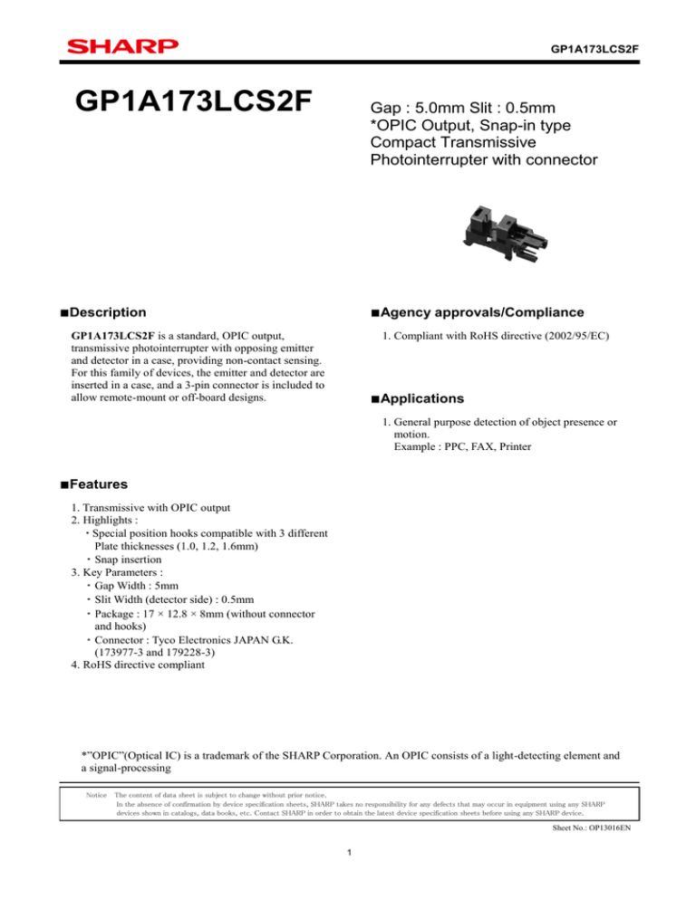
GP1A173LCS2F
GP1A173LCS2F
Gap : 5.0mm Slit : 0.5mm
*OPIC Output, Snap-in type
Compact Transmissive
Photointerrupter with connector
■Description
■Agency approvals/Compliance
GP1A173LCS2F is a standard, OPIC output,
transmissive photointerrupter with opposing emitter
and detector in a case, providing non-contact sensing.
For this family of devices, the emitter and detector are
inserted in a case, and a 3-pin connector is included to
allow remote-mount or off-board designs.
1. Compliant with RoHS directive (2002/95/EC)
■Applications
1. General purpose detection of object presence or
motion.
Example : PPC, FAX, Printer
■Features
1. Transmissive with OPIC output
2. Highlights :
・Special position hooks compatible with 3 different
Plate thicknesses (1.0, 1.2, 1.6mm)
・Snap insertion
3. Key Parameters :
・Gap Width : 5mm
・Slit Width (detector side) : 0.5mm
・Package : 17 × 12.8 × 8mm (without connector
and hooks)
・Connector : Tyco Electronics JAPAN G.K.
(173977-3 and 179228-3)
4. RoHS directive compliant
*”OPIC”(Optical IC) is a trademark of the SHARP Corporation. An OPIC consists of a light-detecting element and
a signal-processing
Notice
The content of data sheet is subject to change without prior notice.
In the absence of confirmation by device specification sheets, SHARP takes no responsibility for any defects that may occur in equipment using any SHARP
devices shown in catalogs, data books, etc. Contact SHARP in order to obtain the latest device specification sheets before using any SHARP device.
Sheet No.: OP13016EN
1
GP1A173LCS2F
■Internal Connection Diagram
① Vcc
② Vout
③ GND
■Outline
Drawing No. CY14233i02B
Scale : 2/1
Unit : 1/1 mm
Note) 1. Unspecified tolerance shall be followed the list below.
2. Dimensions in parenthesis are shown for reference.
3. Coupling and contact : CT receptacle connector
(173977-3 and 179228-3) by Tyco Electronics Japan G.K.
Dimension
less than 5.0
5.0 or more less than 15.0
15.0 or more
Tolerance
±0.15
±0.2
±0.3
Sheet No.: OP13016EN
2
GP1A173LCS2F
■Absolute maximum ratings
Ta=25°C
Parameter
Symbol
Rating
Unit
Supply voltage
Vcc
-0.5 to +7
V
Output voltage
Vout
-0.5 to +7
V
Output current
IOL
Operating temperature
Topr
8
-30 to +95
Remark
Output transistor between collector and emitter
mA
Output transistor collector current
*1
°C
The connector should be plugged in/out
at normal temperature.
Storage temperature
Tstg
-40 to +100
°C
*1 Fig.1 shows output current vs. ambient temperature.
■Electro-optical Characteristics
Vcc=5V, Ta=25°C
Parameter
Symbol
Current consumption
ICCL
VOL
Low level output voltage
Current consumption
ICCH
VOH
High level output voltage
Operating voltage
Vcc
Min. interrupted
tH
Response
time
characteristics
Min. uninterrupted
tL
time
Rating
Conditions
Unit
16.5 MAX.
Light beam uninterrupted
Light beam uninterrupted
IOL=4mA
mA
V
0.35 MAX
16.5 MAX
Vcc×0.9 MIN
4.5 to 5.5
mA
Light beam interrupted
V
Light beam interrupted
RL=47kΩ
V
μs
166 MIN
RL=4.7kΩ
μs
166 MIN
■Detection position characteristics
Ta=25°C, Vcc=5V, RL=47kΩ
Vertical detecting position characteristics
(d = 3.0 +0.3 mm)
Horizontal detecting position characteristics
(d = 3.2±0.3mm)
0
1
2
3
4
5
Distance d (mm)
Shield
d
6
-1.8
Output”High”
Output”High”
Output”Low”
Output”Low”
7
0
1
2
3
4
5
6
Distance d (mm)
0
Shield
0
d
Sheet No.: OP13016EN
3
GP1A173LCS2F
Fig.1 Output current vs. ambient temperature
10
Output current IOL [mA]
8
6
4
2
0
-30
-15
0
15
30
45
60
75
90
105
Ambient temperature Ta [℃]
Sheet No.: OP13016EN
4
GP1A173LCS2F
■Supplements
●ODS materials
This product shall not contain the following materials.
Also, the following materials shall not be used in the production process for this product.
Materials for ODS : CFCS, Halon, Carbon tetrachloride 1.1.1-Trichloroethane (Methyl chloroform)
●Specified brominated flame retardants
Specified brominated flame retardants (PBB and PBDE) are not used in this device at all.
●Compliance with each regulation
1) The RoHS directive(2002/95/EC)
This product complies with the RoHS directive(2002/95/EC).
Object substances: mercury, lead, cadmium, hexavalent chromium, polybrominated biphenyls (PBB)
and polybrominated diphenyl ethers (PBDE)
2) Content of six substances specified in Management Methods for Control of Pollution Caused by Electronic
Information Products Regulation (Chinese : 电子信息产品污染控制管理办法).
Toxic and hazardous substances
Hexavalent
Polybrominated
Polybrominated
Category
Lead
Mercury Cadmium
chromium
biphenyls
diphenyl ethers
(Pb)
(Hg)
(Cd)
(Cr6+)
(PBB)
(PBDE)
Photointerrupter
✓
✓
✓
✓
✓
✓
✓: indicates that the content of the toxic and hazardous substance in all the homogeneous materials of the part is
below the concentration limit requirement as described in SJ/T 11363-2006 standard.
●Product mass : Approx. 1.0g
●Country of origin : Philippine or China
Sheet No.: OP13016EN
5
GP1A173LCS2F
■Notes
●Truth Table (In case of external addition pull-up resistance to Vout terminal)
Light beam
Output
Interrupted
High
Uninterrupted
Low
●Power supply line
In order to stabilize power supply line, connect a by-pass capacitor of more than 0.01μF between Vcc
and GND near the device.
●Opaque board
Opaque board shall be installed at place 4mm or more from the top of elements.
(Example)
4mm or more
In case opaque board is the material with an low light blocking effect, There is a possibility of malfunctioning
because the light of LED transmits the opaque board. When you design the opaque board, please note transmittance
of infrared rays wave length (950nm) and the thickness of the opaque board.
And, please adjust the amount of transmitted light to 0.1% or less.
●Cleaning
Please don't carry out immersion cleaning or ultrasonic cleaning to avoid keeping solvent inside case of this device.
●Washing material
Dust and stain shall clean by air blow, or shall clean by soft cloth soaked in washing materials.
And washing material to clean shall be used the below materials only.
Ethyl alcohol, Methyl alcohol, Isopropyl alcohol
●Connector connection
For the electrical connection to the connector terminal, please certainly use the connector specified in this
specifications.
Please avoid the connection by the soldering or welding which may damage the main body of the device,
and also avoid the contact by the clip and so on which may cause the malfunction by the contact failure.
Please avoid the use condition that t it always occurs he vibration in the spot where the connector fits in
by the resonance of the sensor and the harness.
It may cause the malfunction of the contact failure.
●Put-in and pull-out of connector
The connection other than to the correct connection direction, forcing-into, and the pulling-out diagonally
(if being not put-in and pulled-out straight) may deform or break the connector terminal and/or housing,
which may cause the unusable state of the device.
●Interference light
Because the upper, bottom and “Date Code” side are not covered by outer case,
please do not use this device under ambient light circumstances including infrared component.
Sheet No.: OP13016EN
6
GP1A173LCS2F
■Recommended Installation Hole drawing
Scale : 2/1
Unit : 1/1mm
(Drawing No. CY14234i06A)
*1
*2
*3
*4
We recommend to fix GP1A173LCS2F at punching side on the fixing plate (metal plate).
Please decide the final dimensions at your side after confirmation by the actual
applications, Because mounting efficiency and mounted stabilization are dependent
on mounting plate corner-R and punched state.
Tolerance shall be ±0.1mm
Please don’t hold connector area but sensor area when fitting in or putting out on the metal plate.
Normal mounting type
Thickness of plate for 1.6mm
Thickness of plate for 1.2mm
Thickness of plate for 1.0mm
Irregular mounting protection type
Thickness of plate for 1.6mm
Thickness of plate for 1.2mm
Thickness of plate for 1.0mm
Sheet No.: OP13016EN
7
GP1A173LCS2F
■Parts
This product uses the following parts.
● Light detector (Quantity : 1)
(Using a silicon photodiode as light detecting portion, and a bipolar IC as signal processing circuit.)
Type
Maximum sensitivity
wavelength (nm)
Sensitivity
wavelength (nm)
Response time
(μs)
Photodiode
900
400 to 1200
10
● Light emitter (Quantity : 1)
Type
Material
Maximum light emitting
wavelength (nm)
I/O Frequency
(MHz)
Infrared light
emitting diode
(non-coherent)
GaAs
950
0.3
● Material
Case
Lead flame
Black polycarbonate resin
(UL 94V-0)
Copper Alloy
(With plating)
● Others
This product shall not be radiation flux proof.
The laser oscillator is not equipped on this product.
The terminals are covered with Tin Plating (more than 99.99%).
Sheet No.: OP13016EN
8
GP1A173LCS2F
■Packing specification
● Package
No.
1
2
3
4
Name
Packing case
Pad
Tray
Kraft tape
Material
Corrugated cardboard
Corrugated cardboard
Polystyrene
Quantity
1/1000
6/1000
1/200
-
● Packing method
1) 5 products are put in 1 pocket.
The longer direction of the product is arranged in the arbitrary direction.
200 products are put in the tray. <Fig.1>
2) The pads are attached at the top and the bottom of the trays and also inserted between the trays. <Fig.2>
3) Seal packing case with Kraft tape. <Fig.3>
4) Indication items
The contents of the carton indication conforms to EIAJ C-3 and the following items are indicated.
Model No., Internal production control name, Quantity, Packing date, Corporate name,
Country of origin <Fig.3>
(1000pcs. / packing case)
(Approximately 2.26kg / packing mass)
Sheet No.: OP13016EN
9
GP1A173LCS2F
■Important Notices
· The circuit application examples in this publication are provided
to explain representative applications of SHARP devices and are
not intended to guarantee any circuit design or license any
intellectual property rights. SHARP takes no responsibility for
any problems related to any intellectual property right of a third
party resulting from the use of SHARP's devices.
with equipment that requires higher reliability such as:
--- Transportation control and safety equipment (i.e.,
aircraft, trains, automobiles, etc.)
--- Traffic signals
--- Gas leakage sensor breakers
--- Alarm equipment
--- Various safety devices, etc.
(iii) SHARP devices shall not be used for or in connection with
equipment that requires an extremely high level of reliability and
safety such as:
--- Space applications
--- Telecommunication equipment [trunk lines]
--- Nuclear power control equipment
--- Medical and other life support equipment (e.g.,
scuba).
· Contact SHARP in order to obtain the latest device specification
sheets before using any SHARP device. SHARP reserves the
right to make changes in the specifications, characteristics, data,
materials, structure, and other contents described herein at any
time without notice in order to improve design or reliability.
Manufacturing locations are also subject to change without
notice.
· Observe the following points when using any devices in this
publication. SHARP takes no responsibility for damage caused
by improper use of the devices which does not meet the
conditions and absolute maximum ratings to be used specified in
the relevant specification sheet nor meet the following
conditions:
(i) The devices in this publication are designed for use in general
electronic equipment designs such as:
--- Personal computers
--- Office automation equipment
--- Telecommunication equipment [terminal]
--- Test and measurement equipment
--- Industrial control
--- Audio visual equipment
--- Consumer electronics
(ii) Measures such as fail-safe function and redundant design
should be taken to ensure reliability and safety when SHARP
devices are used for or in connection
· If the SHARP devices listed in this publication fall within the
scope of strategic products described in the Foreign Exchange
and Foreign Trade Law of Japan, it is necessary to obtain
approval to export such SHARP devices.
· This publication is the proprietary product of SHARP and is
copyrighted, with all rights reserved. Under the copyright laws,
no part of this publication may be reproduced or transmitted in
any form or by any means, electronic or mechanical, for any
purpose, in whole or in part, without the express written
permission of SHARP. Express written permission is also
required before any use of this publication may be made by a
third party.
· Contact and consult with a SHARP representative if there are
any questions about the contents of this publication.
Sheet No.: OP13016EN
10


