IJSRD - International Journal for Scientific Research & Development| Vol. 3, Issue 03, 2015 | ISSN (online): 2321-0613
Simulation and Analysis of Parallel Resonant DC Link Inverter
Piyush V. Shingala1 Alpesh S. Adesara2
2
Professor
1,2
Department of Electrical Engineering
1,2
V.V.P. Engineering College, Rajkot, India
Abstract— parallel resonant dc link that provides soft
switching and pulse width modulated inverter is presented.
The new PRDCL ensures zero crossing of time period.
Key words: Soft switching , Parallel resonant dc link
inverter, PWM.
I. INTRODUCTION
Induction motors with squirrel-cage rotors are found in
numerous industrial applications because of their low cost
and rugged construction. When induction motors are
operated directly from the line voltage,they run at a nearly
constant speed, determined by the line voltage frequency
and the number of poles in the machine.
Power conversion is required to effectively and
efficiently control motors of all kind. Performance of the
overall system is greatly dependent on the appropriate
conversion and power to the motor. For example, a system
could utilize the most efficient motor and still operate very
inefficiently if the motor is not driven properly. Significant
improvement can be made in the efficiency; power density
and reliability of present motor drives by using new
topologies operates at higher switching speeds and employ
new control strategies that lead to enhance the performance.
Resonant inverter is the generic name for a type of high
frequency switching topology used in many of Spellman's
supplies. Resonant switching topologies are the next
generation of power conversion circuits, when compared to
traditional pulse width modulation (PWM) topologies.
Resonant-based supplies are more efficient than their PWM
counterparts. This is due to the zero current and/or zero
voltage transistors switching that is inherent in a resonant
supplies design. This feature also provides an additional
benefit of eliminating undesirable electromagnetic radiation
normally associated with switching supplies.
II. PROBLEM IDENTIFICATION
Usually electric vehicles utilize hard switching inverters
(HSI) to drive their motors. The attractiveness of the hard
switching inverter stems from its circuit simplicity and
rugged control schemes. However, this type of inverter
suffers from high switching losses, high switching stresses,
and EMI (electromagnetic interference) problems. To solve
these problems, soft switching resonant dc link inverters
have been proposed. In a Resonant DC link inverter, the dc
bus is controlled to oscillate at a high frequency so that the
bus voltage goes through periodic zero crossings, thus
setting up zero voltage switching conditions for all devices
across the bus. The resonant dc link inverter has been shown
to be a viable topology to realize high performance and high
power density ac drives.
III. SOFT SWITCHING
Traditional hard-switching inverters presented several
problems during switching. During turn-on, the device
current rises from zero to the load current with additional
diode reverse recovery and stray capacitor charging and
discharging currents on top of the load current.Typically, a
current spike will occur, and the peak device power
consumption is extremely high. Duringturn-off, the device
voltage rises. Due to the leakage inductance intheloop,
avoltage over shoot caused by Ldi/dt will occur, and the
device voltage will exceed the dc bus voltage. This voltage
over shoot can be reduced by a good circuit layout and high
frequency DC bus capacitors. The turn-off loss varies
among different types of devices depending upon the turnoff delay and current fall time. The Power MOSFET
consumes least turn-off loss. The insulated gate bipolar
transistor(IGBT) turn-off loss also varies among different
manufacturing processes and its associated minority carrier
life time killing. Some ultrafast IGBTs may have low turnoff lossc lose to that of power MOSFETs. The bipolar
junction transistors(BJTs), in general, have along turn-off
delay time and consequently, high switching losses.
Another switching problem is the voltage rise and fallrate,
di/dt .During turn-on, the voltage falls to zero when the
opposite switch turns on.During turn-off, the voltage rises
to the dc bus voltage with an overshoot.
IV. SOFTSWITCHINGDC ACCONVERTERS
Thedevelopmentofsoftswitchinginvertersforacmotors(includinginductionmotors,P
MbrushlessmotorsandPMhybridmotorsbecomearesearchdirec
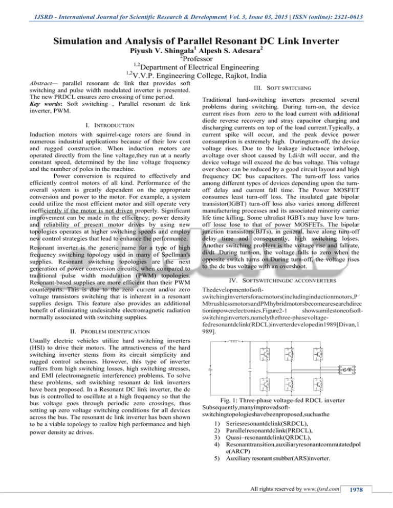
tioninpowerelectronics.Figure2-1
showsamilestoneofsoftswitchinginverters,namelythethree-phasevoltagefedresonantdclink(RDCL)inverterdevelopedin1989[Divan,1
989].
Fig. 1: Three-phase voltage-fed RDCL inverter
Subsequently,manyimprovedsoftswitchingtopologieshavebeenproposed,suchasthe
1)
2)
3)
4)
Seriesresonantdclink(SRDCL),
Parallelresonantdclink(PRDCL),
Quasi–resonantdclink(QRDCL),
Resonanttransition,auxiliaryresonantcommutatedpol
e(ARCP)
5) Auxiliary resonant snubber(ARS)inverter.
All rights reserved by www.ijsrd.com
1978
Simulation and Analysis of Parallel Resonant DC Link Inverter
(IJSRD/Vol. 3/Issue 03/2015/492)
V. PROPOSED SCHEME:-
VII. SIMULATION
A. Block diagram
Figure 2. shows the block diagram forParallel Resonant DC
Link inverter. As shown in figure DC supply is given to the
DC links which constitute an inductor and capacitor in
parallel. The output of DC link is given to the three phase
PWM VSI. The switching losses in a PWM inverter is
avoided by connecting a resonant circuit in between the DC
input voltage and the PWM inverter. The output of PWM
inverter is given to the three phase induction motor. Control
circuit for DC link and three phases PWM VSI are
connected.
DC
SUPPLY
DC
LINK
THREE
PHASEPWM
VSI
INDUCTION
MOTOR
Fig 4: Simulation of PRDCL inverter with R load.
Simulation of Parallel Resonant DC Link Inverter with R
load is prepared by MATLAB 2010a as shown in fig.4
Scopes are connected to measure three phase output line
voltage VL, Phase voltage VP and output current Io. Fig. 5.2
shows a simulation result of three phase output line voltage
VL, Phase voltage VP and output current Io with R load.
VIII. RESULTS
CONTROL
SWITCH FOR DC
LINK & SWITCH
CONTROL
CIRCUIT FOR
INVERTER
Fig. 2: Block diagram of proposed scheme
VI. OPERATING PRINCIPLE
This topology involves placing a simple L-C resonant circuit
between the DC bus and a conventional inverter. The
PRDCL Inverter operates in the following manners. A DC
voltage is applied to a parallel L-C resonant circuit with a
switch S across the capacitor. By closing switch, the
inductor is charged. When inductor is charged to a sufficient
level switch is opened and the resonant bus voltage
oscillates and returns to zero. The resonant switch is closed
every time the resonant bus voltage returns to zero. At this
time the power switching devices in the inverter bridge are
turned on or off ensuring a zero voltage transition.
Fig. 6: Results
Fig.7: Simulation of PRDCL with RL load
Fig 3. Parallel Resonant DC Link Inverter
Simulation of Parallel Resonant DC Link Inverter with RL
load is prepared by MATLAB 2010a as shown in figure 5.5.
Scopes are connected to measure three phase output line
voltage VL, Phase voltage VP and output current Io. Figure
5.6 shows a simulation result of three phase output line
voltage VL, Phase voltage VP and output current Io with RL
load.
All rights reserved by www.ijsrd.com
1979
Simulation and Analysis of Parallel Resonant DC Link Inverter
(IJSRD/Vol. 3/Issue 03/2015/492)
Fig. 8: Results
IX. HARDWARE
Fig 11 Dc Link and Supply circuit
X. PARAMETERS USED IN HARDWARE
Input voltage :- 230 V AC
Inductor :- 45 milihenry
Capacitor :- 0.8 microfarad
DC link frequency :- 20Khz
Switching frequency :- 5Khz
Ratings of Motor:-3 phase,230 volt,1.3 Amp,0.25
hp.
Microcontroller :- 89C51
Transformer :- 230/24 volts,5 Amp and 230/24
volts, 1.5 Amp
Fig. 9: Hardware Setup
XI. CONCLUSION
Fig. 10: Control Circuit
In this project report, PRDCL circuit is presented. This
circuit provides zero crossings on the DC link to implement
the SS and PWM operation of the inverters.The new circuit
combines the most desirable features and overcomes most
drawbacks of other circuits using only one auxiliary switch.
Subsequently, all semiconductor devices in the circuit
operate under SS, the circuit can successfully operate under
various load conditions.
A resonant DC link inverter driving a0.18kW
induction motor for an electric vehicle application has been
developed. Inverter operation with an 110V DC supply at a
link frequency of approximately 20 KHz has been
successfully demonstrated. It has been experimentally
checked that the resonant DC link inverter is capable of bidirectional power flow. Inverter tests have shown that the
resonant DC link inverter has the advantages of low losses,
allow dv/dt, low acoustic noise, a high switching frequency,
and snubber less operation. Therefore, the resonant DC link
inverter has a promising application to electric vehicle
propulsion.
All rights reserved by www.ijsrd.com
1980
Simulation and Analysis of Parallel Resonant DC Link Inverter
(IJSRD/Vol. 3/Issue 03/2015/492)
REFERENCES
[1] Zhenyue Hong, Richard Duke, Simon Round, “A
RESONANT DC LINK INVERTER FOR AN
ELECTRIC VEHICLE,” Department of Electrical and
Electronic Engineering University of Canterbury, New
Zealand,2011.
[2] Giri Venkataramanan, D.M.Divan, “Pulse Width
Modulation with Resonant dc Link Converters,” IEEE
TRANSACTIONS ON INDUSTRY APPLICATIONS,
VOL. 29, NO. 1, JANUARYFEBRUARY,1993.
[3] T. W. Ching, “Soft-switching Converters for Electric
Vehicle
Propulsion,”Department of
Electromechanical Engineering, University of Macau.
DECEMBER,2007.
[4] HULYA
OBDAN,HACI
BODUR
,ISMAIL
AKSOY,NUR
BEKIROGLU,GULDEREN
YILDIRMAZ, “A New Parallel Resonant DC Link for
Soft Switching Inverters.” Yildiz Technical University
Besiktas, Istanbul, Turkey, December,2003.
[5] Bill Andreycak, “Zero Voltage Switching Resonant
Power Conversion,” IEEE TRANSACTIONS ON
INDUSTRY APPLICATION,2011.
All rights reserved by www.ijsrd.com
1981
