< HVIC >
M81740FP
HIGH VOLTAGE HALF BRIDGE DRIVER
DESCRIPTION
M81740FP is high voltage Power MOSFET and IGBT
gate driver for half bridge applications.
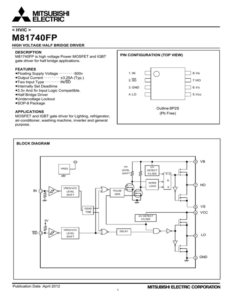
PIN CONFIGURATION (TOP VIEW)
FEATURES
●Floating Supply Voltage ・・・・・・・・600v
●Output Current ・・・・・・・・ ±3.25A (Typ.)
●Two Input Type ・・・・・・・・IN/SD
●Internally Set Deadtime
●3.3v And 5v Input Logic Compartible.
●Half Bridge Driver
●Undervoltage Lockout
●SOP-8 Package
1. IN
8.V B
2. SD
7.HO
3. GND
6.V S
4. LO
5.Vcc
Outline:8P2S
(Pb Free)
APPLICATIONS
MOSFET and IGBT gate driver for Lighting, refrigerator,
air-conditioner, washing machine, inverter and general
purpose.
BLOCK DIAGRAM
HV
LEVEL
SHIFT
VREG
IN
INTER
LOCK
VREG/VCC
LEVEL
SHIFT
1
UV
DETECT
FILTER
7
HO
6
VS
5
VCC
4
LO
3
GND
RQ
R
S
UV DETECT
FILTER
5V
2
VB
PULSE
GEN
DEAD
TIME
SD
8
VREG/VCC
LEVEL
SHIFT
DELAY
Publication Date :April 2012
1
<HVIC>
M81740FP
HIGH VOLTAGE HALF BRIDGE DRIVER
TYPICAL CONNECTION ( General Purpose)
up to 600V
Vcc
To
Controller
VCC
VB
IN
HO
SD
VS
COM
LO
To
Load
Publication Date : April 2012
2
<HVIC>
M81740FP
HIGH VOLTAGE HALF BRIDGE DRIVER
TYPICAL CONNECTION ( In Unipolar Modulation PWM Application)
up to 600V
IC1
IC2
SD
Vs
HO
Ua
Load
LO
Ub
Vs
LO
SEQUENCE ( SD is used as low side input terminal)
IC1_IN
IC1_SD
IC2_IN
IC2_SD
IC1_HO
IC1_LO
IC2_HO
IC2_LO
Ua - Ub
Publication Date : April 2012
3
M81740FP
IN
M81740FP
HO
IN
SD
<HVIC>
M81740FP
HIGH VOLTAGE HALF BRIDGE DRIVER
ABSOLUTE MAXIMUM RATINGS (Ta=25°C unless otherwise specified)
Symbol
VB
VS
VBS
VHO
VCC
VLO
Parameter
Test conditions
VIN
High Side Floating Supply Absolute Voltage
High Side Floating Supply Offset Voltage
High Side Floating Supply Voltage
High Side Output Voltage
Low Side Fixed Supply Voltage
Low Side Output Voltage
Logic Input Voltage (IN & SD)
dVS/dt
Pd
Kθ
Rth(j-c)
Tj
Topr
Tstg
TL
Allowable Offset Voltage Transient
Package Power Dissipation
Linear Derating Factor
Junction-Case Thermal Resistance
Junction Temperature
Operation Temperature
Storage Temperature
Solder Heatproof
VBS=VB-VS
Ta= 25 °C ,On Board
Ta> 25 °C ,On Board
RoHS Correspondence
Ratings
Unit
-0.3 ~ 624
VB-24 ~ VB+0.3
-0.3 ~ 24
VS-0.3 ~ VB+0.3
-0.3 ~ 24
-0.3 ~ Vcc+0.3
V
V
V
V
V
V
-0.3 ~ Vcc+0.3
V
±50
0.6
4.8
50
-40 ~ +150
-40 ~ +125
-50 ~ +150
255:10s,max 260
V/ns
W
mW/°C
°C/W
℃
℃
℃
℃
RECOMMENDED OPERATING CONDITIONS
Symbol
VB
VS
VBS
VHO
VCC
VLO
VIN
Parameter
Test conditions
High Side Floating Supply Absolute Voltage
High Side Floating Supply Offset Voltage
High Side Floating Supply Voltage
High Side Output Voltage
Low Side Fixed Supply Voltage
Low Side Output Voltage
Logic Input Voltage (IN & SD)
VB>10V
VBS=VB-VS
Min.
VS+10
-5
10
VS
10
0
0
* For proper operation, the device should be used within the recommended conditions
Package Power Dissipation Pd (W)
THERMAL DERATING FACTOR CHARACTERISTIC (MAXIMUM RATING)
0.7
0.6
0.5
0.4
0.3
0.2
0.1
0
0
25
50
75
100 125 150
Temperature Ta(oC)
Publication Date : April 2012
4
Limits
Typ.
—
—
—
—
—
—
—
Max.
VS+20
500
20
VB
20
VCC
5
Unit
V
V
V
V
V
V
V
<HVIC>
M81740FP
HIGH VOLTAGE HALF BRIDGE DRIVER
ELECTRICAL CHARACTERISTICS (Ta=25°C,VCC=VBS(=VB-VS)=15V, unless otherwise specified)
Symbol
Min.
—
—
0.2
13.8
—
—
0.8
—
0.8
—
—
7.0
0.3
—
7.0
0.3
—
Limits
Typ.*
—
0.2
0.6
14.4
—
2.2
1.6
2.2
1.6
25
—
8.4
0.5
7.5
8.4
0.5
7.5
Max.
1.0
0.5
1.0
—
0.2
2.7
—
2.7
—
60
5
9.8
—
—
9.8
—
—
VO = 0V, PW < 10s
2.3
3.25
—
A
VO = 15V, PW < 10s
2.3
3.25
—
A
—
—
900
ns
—
—
400
ns
—
—
—
—
—
—
—
—
0
0
—
—
—
—
270
90
40
60
35
60
35
ns
ns
ns
ns
ns
ns
ns
280
400
520
ns
—
0
50
ns
Parameter
IFS
IBS
ICC
VOH
VOL
VIH(IN)
VIL(IN)
VIH(SD)
VIL(SD)
IIH
IIL
VBSuvr
VBSuvh
tVBSuv
VCCuvr
VCCuvh
tVCCuv
Test conditions
Floating Supply Leakage Current
VBS Standby Current
VCC Standby Current
High Level Output Voltage
Low Level Output Voltage
High Level Input Threshold Voltage (VIN)
Low Level Input Threshold Voltage (VIN)
High Level Input Threshold Voltage (VSD)
Low Level Input Threshold Voltage (VSD)
High Level Input Bias Current
Low Level Input Bias Current
VBS Supply UV Reset Voltage
VBS Supply UV Hysteresis Voltage
VBS Supply UV Filter Time
VCC Supply UV Reset Voltage
VCC Supply UV Hysteresis Voltage
VCC Supply UV Filter Time
Output High Level Short Circuit Pulsed
Current
Output Low Level Short Circuit Pulsed
Current
IOH
IOL
tdLH
Turn-On Propagation Delay
tdHL
Turn-Off Propagation Delay
VB = VS = 600V
IN = 0V or 5V
IN = 0V or 5V
IO = 0mA, LO, HO
IO = 20mA, LO, HO
VIN = 5V ,VSD=0V
VIN = 0V ,VSD=5V
CL = 1000pF between HO-VS, LO-GND
VIN = 0~5V
CL = 1000pF between HO-VS , LO-GND
VIN = 0~5V
Shut Down Propagation Delay
Turn-On Propagation Delay Matching
Turn-Off Propagation Delay Matching
High Side Turn-On Rise Time
High Side Turn-Off Fall Time
Low Side Turn-On Rise Time
Low Side Turn-Off Fall Time
Dead Time LO Turn-Off to HO Turn-On &
tDEAD
HO Turn-Off to LO Turn-On
⊿tDEAD Dead Time Matching
tSD
⊿tdLH
⊿tdHL
trH
tfH
trL
tfL
|tdLH(HO)-tdLH(LO)|
|tdHL(HO)-tdHL(LO)|
CL = 1000pF between HO-VS
CL = 1000pF between HO-VS
CL = 1000pF between LO-GND
CL = 1000pF between LO-GND
CL = 1000pF between HO-VS, LO-GND
VIN = 0~5V
|tDEAD(LO-HO)-tDEAD(HO-LO)|
* Typ. is not specified.
INPUT/OUTPUT TIMING DIAGRAM
IN
50%
SD
50%
trH
tfL
tfH
90%
trL
90%
10%
10%
tSD
90%
HO
LO
HO
90%
90%
LO
tdHL(LO)
tdLH(HO)
10%
tDEAD
(LO-HO)
10%
tDEAD
(HO-LO)
tdHL(HO)
tdLH(LO)
Publication Date : April 2012
5
50%
Unit
A
mA
mA
V
V
V
V
V
V
A
A
V
V
s
V
V
s
<HVIC>
M81740FP
HIGH VOLTAGE HALF BRIDGE DRIVER
FUNCTION TIMING DIAGRAM 1
IN
SD
HO
LO
FUNCTION TIMING DIAGRAM 2
UVreset
Vcc
UVreset
UV trip
UV trip
UV reset voltage
UV trip voltage
UV trip
UVreset
UVreset
UV reset voltage
UV trip voltage
VB
UV reset voltage
UV trip voltage
IN
tVBSuv
tVccuv
HO
tVccuv
LO
Publication Date : April 2012
6
<HVIC>
M81740FP
HIGH VOLTAGE HALF BRIDGE DRIVER
1. HO has positive logic with reference to IN. LO has negative logic with reference to IN.
2. Output signal (HO) is triggered by the edge of input signal.
3. Logic During UV(VCC, VBS) Error
Error Signal
UV error
(VCC)
HO
LO
HO is locked at “L” level as long as UV error for VCC is
detected. After VCC exceeds VCC UV reset level, the
lock for HO is removed and responds to IN signal.
LO is locked at “L” level as long as UV error for VCC is
detected. After VCC exceeds VCC UV reset level, the lock
for LO is removed and responds to IN signal.
(VCC>VBS)
UV error
(VBS)
HO is locked at “L” level as long as UV error for VBS is
detected. After VBS UV reset level, the lock for HO is
removed following an “L” state of the IN signal, and
then HO responds to the input.
LO is independent of VBS to respond to IN.
*IF UV error for VCC is detected when HO is in “H” level and the falling speed of VCC is exceeds 0.03V/μs, the off signal for HO might
not be transmitted from low side to high side and then HO stays “H”.
4. Supply start up sequence
Please start up VCC supply and VBS supply in that order, and, please shut down VBS supply and VCC supply in that
order. Please start up VCC supply and VBS supply with gentle slope. If you start up supply with sharp slope, there is
some possibility that HO or LO outputs “H” for a moment.
If VCC supply is less than 10V(outside of RECOMMENDED OPERATING CONDITIONS), there is some possibility that
output does not change in response to input. Please evaluate carefully about supply start up or restart after shut down
in your application systems.
Publication Date : April 2012
7
<HVIC>
M81740FP
HIGH VOLTAGE HALF BRIDGE DRIVER
PACKAGE OUTLINE
Publication Date : April 2012
8
<HVIC>
M81740FP
HIGH VOLTAGE HALF BRIDGE DRIVER
Main Revision for this Edition
Revision
No.
Date
Pages
Points
A
2012.01.26
-
New
B
2012.04.10
-
“PRELIMINARY” was deleted.
“Notice: This is not a final specification.
Some parametric limits are subject to change.” was deleted.
4
“Storage Temperature” was changed to “-50 ~ +150 ℃”.
5
Min. and Max. Limits of tDEAD was added.
Publication Date : April 2012
9
<HVIC>
M81740FP
HIGH VOLTAGE HALF BRIDGE DRIVER
Keep safety first in your circuit designs!
Mitsubishi Electric Corporation puts the maximum effort into making semiconductor products better and more
reliable, but there is always the possibility that trouble may occur with them. Trouble with semiconductors
may lead to personal injury, fire or property damage. Remember to give due consideration to safety when
making your circuit designs, with appropriate measures such as (i) placement of substitutive, auxiliary
circuits, (ii) use of non-flammable material or (iii) prevention against any malfunction or mishap.
Notes regarding these materials
•These materials are intended as a reference to assist our customers in the selection of the Mitsubishi
semiconductor product best suited to the customer’s application; they do not convey any license under
any intellectual property rights, or any other rights, belonging to Mitsubishi Electric Corporation or a third
party.
•Mitsubishi Electric Corporation assumes no responsibility for any damage, or infringement of any thirdparty’s rights, originating in the use of any product data, diagrams, charts, programs, algorithms, or
circuit application examples contained in these materials.
•All information contained in these materials, including product data, diagrams, charts, programs and
algorithms represents information on products at the time of publication of these materials, and are
subject to change by Mitsubishi Electric Corporation without notice due to product improvements or
other reasons. It is therefore recommended that customers contact Mitsubishi Electric Corporation or an
authorized Mitsubishi Semiconductor product distributor for the latest product information before
purchasing a product listed herein.
The information described here may contain technical inaccuracies or typographical errors. Mitsubishi
Electric Corporation assumes no responsibility for any damage, liability, or other loss rising from these
inaccuracies or errors.
Please also pay attention to information published by Mitsubishi Electric Corporation by various means,
including the Mitsubishi Semiconductor home page (http://www.MitsubishiElectric.com/).
•When using any or all of the information contained in these materials, including product data, diagrams,
charts, programs, and algorithms, please be sure to evaluate all information as a total system before
making a final decision on the applicability of the information and products. Mitsubishi Electric
Corporation assumes no responsibility for any damage, liability or other loss resulting from the
information contained herein.
•Mitsubishi Electric Corporation semiconductors are not designed or manufactured for use in a device or
system that is used under circumstances in which human life is potentially at stake. Please contact
Mitsubishi Electric Corporation or an authorized Mitsubishi Semiconductor product distributor when
considering the use of a product contained herein for any specific purposes, such as apparatus or
systems for transportation, vehicular, medical, aerospace, nuclear, or undersea repeater use.
•The prior written approval of Mitsubishi Electric Corporation is necessary to reprint or reproduce in
whole or in part these materials.
•If these products or technologies are subject to the Japanese export control restrictions, they must be
exported under a license from the Japanese government and cannot be imported into a country other
than the approved destination.
Any diversion or re-export contrary to the export control laws and regulations of Japan and/or the
country of destination is prohibited.
•Please contact Mitsubishi Electric Corporation or an authorized Mitsubishi Semiconductor product
distributor for further details on these materials or the products contained therein.
© 2012 MITSUBISHI ELECTRIC CORPORATION. ALL RIGHTS RESERVED.
Publication Date : April 2012
10


