application bulletin
advertisement

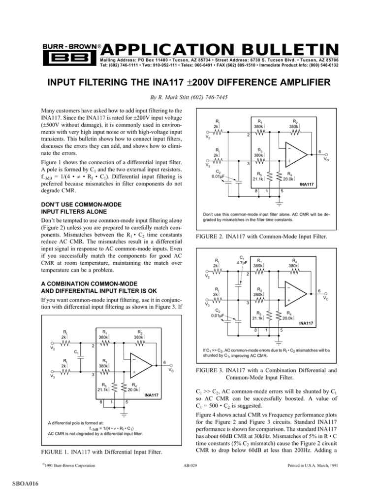
APPLICATION BULLETIN ® Mailing Address: PO Box 11400 • Tucson, AZ 85734 • Street Address: 6730 S. Tucson Blvd. • Tucson, AZ 85706 Tel: (602) 746-1111 • Twx: 910-952-111 • Telex: 066-6491 • FAX (602) 889-1510 • Immediate Product Info: (800) 548-6132 INPUT FILTERING THE INA117 ±200V DIFFERENCE AMPLIFIER By R. Mark Stitt (602) 746-7445 Many customers have asked how to add input filtering to the INA117. Since the INA117 is rated for ±200V input voltage (±500V without damage), it is commonly used in environments with very high input noise or with high-voltage input transients. This bulletin shows how to connect input filters, discusses the errors they can add, and shows how to eliminate the errors. RI 2kΩ R2 380kΩ 2 V2 RI 2kΩ Figure 1 shows the connection of a differential input filter. A pole is formed by C1 and the two external input resistors. f–3dB = 1/(4 • π • RI • C1). Differential input filtering is preferred because mismatches in filter components do not degrade CMR. DON’T USE COMMON-MODE INPUT FILTERS ALONE Don’t be tempted to use common-mode input filtering alone (Figure 2) unless you are prepared to carefully match components. Mismatches between the RI • C2 time constants reduce AC CMR. The mismatches result in a differential input signal in response to AC common-mode inputs. Even if you successfully match the components for good AC CMR at room temperature, maintaining the match over temperature can be a problem. R1 380kΩ R3 380kΩ 6 VO 3 V3 C2 0.01µF R5 21.1kΩ R4 20.0kΩ INA117 8 1 5 Don’t use this common-mode input filter alone. AC CMR will be degraded by mismatches in the filter time constants. FIGURE 2. INA117 with Common-Mode Input Filter. RI 2kΩ R1 380kΩ R2 380kΩ 2 V2 A COMBINATION COMMON-MODE AND DIFFERENTIAL INPUT FILTER IS OK If you want common-mode input filtering, use it in conjunction with differential input filtering as shown in Figure 3. If C1 4.7µF RI 2kΩ R3 380kΩ 6 VO 3 V3 C2 0.01µF R5 21.1kΩ R4 20.0kΩ INA117 RI 2kΩ R1 380kΩ R3 380kΩ 6 VO 3 R5 21.1kΩ R4 20.0kΩ INA117 8 1 5 A differential pole is formed at: f–3dB = 1/(4 • π • RI • C1) AC CMR is not degraded by a differential input filter. FIGURE 1. INA117 with Differential Input Filter. SBOA016 5 If C1 >> C2, AC common-mode errors due to RI • C2 mismatches will be shunted by C1, improving AC CMR. C1 RI 2kΩ © 1 2 V2 V3 8 R2 380kΩ 1991 Burr-Brown Corporation FIGURE 3. INA117 with a Combination Differential and Common-Mode Input Filter. C1 >> C2, AC common-mode errors will be shunted by C1 so AC CMR can be successfully boosted. A value of C1 = 500 • C2 is suggested. Figure 4 shows actual CMR vs Frequency performance plots for the Figure 2 and Figure 3 circuits. Standard INA117 performance is shown for comparison. The standard INA117 has about 60dB CMR at 30kHz. Mismatches of 5% in R • C time constants (5% C2 mismatch) cause the Figure 2 circuit CMR to drop below 60dB at less than 200Hz. Adding a AB-029 Printed in U.S.A. March, 1991 –100 Standard INA117 –90 CMR117 (dB) ERROR2 (%) INA117BM typ INA117BM min INA117KP min 94 86 70 0.002 0.005 0.033 Fig 3 Circuit TABLE I. Initial INA117 CMR Values. –70 –60 –50 Fig 2 Circuit –40 –30 10 100 1k 10k ERROR1 (%) ERROR2 (%) CMR (dB) 1k 2k 5k 10k 0.005 0.010 0.026 0.051 0.005 0.005 0.005 0.005 80 76 71 65 100k TABLE II. Examples of Worst-Case CMR to be Expected (INA117BM and selected 1% RIs). Frequency (Hz) FIGURE 4. CMR vs Frequency Plots for Figure 2 and 3 Circuits with Standard INA117 for Comparison. ERROR2 = Initial INA117 error [%]—See Table I Also, 4.7µF differential input filter capacitor shunts out commonmode filter errors producing greater than 70dB CMR to 100kHz as shown in the plot of Figure 3’s performance. 105 10(CMR117/20) = Initial INA117 CMR [dB] ERROR2 = CMR117 See Tables I and II for examples. INPUT RESISTORS CAN REDUCE DC CMR Notice that the DC CMR of the Figure 3 circuit is reduced from ≈92dB to ≈82dB. The CMR reduction is due to mismatches from input filter resistors, RI. CMR TRIM If you want to use 10kΩ input resistors and must be assured of good DC CMR, you can use the trim circuit shown in Figure 5. Resistor TCR mismatches can limit difference amplifier performance over temperature. Use high quality film resistors and keep RI ≤ 10kΩ for good performance CMR in the INA117 depends on close resistor ratio matching. For errors in R1 and R3: CMR = –20 Log(%/105) Where: CMR = CMR for errors in R1 or R3 [dB] % = the error in R1 or R3 [%] RI 10kΩ The number, 105, in the denominator comes from R1, R3 sensitivity equations. CMR S R ,R 1 3 RI (Ω) R1 380kΩ 2 V2 C1 = ±R1/(R1 + R4) RI 10kΩ For example, % = 0.002% is required for the typical 94dB INA117 CMR. V3 Even though the 2kΩ input resistors are relatively small compared to the 380kΩ input resistors in the INA117, mismatches will reduce CMR. Even if perfectly matched external input resistors are used there can still be problems with CMR. R2 380kΩ R3 380kΩ 6 VO 3 R5 21.1kΩ R4 20.0kΩ INA117 8 1 5 200Ω CMR Trim 10Ω Although some resistor ratios in the INA117 are carefully matched to achieve good CMR, the R1/R3 ratio is not. A typical mismatch of 1% can be expected. The effect is to add an effective 1% mismatch to external resistors. The following worst-case CMR can be expected: 10Ω CMR (dB) –80 INA117 GRADE CMR = –20 Log((ERROR1 + ERROR2)/105) FIGURE 5. INA117 with Differential Input Filter and CMR Trim. Where: ERROR1 = Error due RI, R1, and R3 mismatches [%] ERROR1 = RI • (TOL + 1)/(RI + 3.8 • 105) RI = DC resistance of external filter resistor, RI, [Ω] TOL = Tolerance of RI [%], i.e. 1.0 for 1% 2 over temperature. mation for all practical purposes. ADDED INPUT RESISTORS CAUSE GAIN ERROR Adding input resistors to the INA117 causes gain error. When all resistor ratios are properly adjusted for good CMR, INA117 gain is R2/R1. When input filter resistors are added, gain is reduced to R2/(RI + R1). With RI = 10kΩ, gain is ≈0.974 V/V (approximately –2.6% gain error). Since gain does not depend on R3, R4, or R5, the gain error can not be corrected by adding resistance in series with any pin. If R2 = 380kΩ, RI = 10kΩ, and R4A = 10Ω: R4B ≈ 180 + R5A ≈ 72MΩ RI ≈ 7.4kΩ , use 7.32kΩ 361 • R2 • R4A • R4B 324(R2 • R4A) + 324(R2 • R4B) – 342(R4A • R4B) With R2 = 380kΩ and R4A = 10Ω: 3.61 • R4B R5A ≈ 3.24 + 0.323991 • R4B CORRECTING GAIN ERROR To correct for the gain error introduced by the input filter resistors, you can add a small amount of positive feedback as shown in Figure 6. Resistors R4A, R4B, and R5A must be selected to maintain CMR and to give the proper positive feedback to correct for gain error. With R4B = 7.4kΩ, R5A = 11.13Ω , use 11Ω. FINE-TRIM FOR ZERO GAIN ERROR You must trim to get zero gain error. The resistors in the INA117 are accurately ratio trimmed to give excellent CMR and gain accuracy, but their absolute values are only accurate to within about ±20%. With the values calculated above, gain error will be reduced from approximately –2.6% to about ±0.5%. The following procedure is suggested: Set R4A = 10Ω This is an arbitrary but adequate value for R4A. It is the smallest standard 1% value. With this small value, even a 5% ratio matching error between R4A and R5A would only degrade INA117 CMR to 82.5dB. In practice, ratio errors will be lower than this when closest standard 1% resistors are used. For lower gain error use the gain-trim circuit shown in Figure 7. The circuit is the same as in Figure 6 except, R4B is replaced with a 5kΩ fixed resistor and a 5kΩ pot. To trim for zero gain error, ground the INA117 inputs (0V input) and measure the offset voltage, VOFF, at the output. Apply a known input voltage, VREF, (e.g. 10.0V) to the INA117 noninverting input. Measure VREF so you know its precise value. Adjust the 5kΩ pot for the correct INA117 Calculate R4B and R5A and use closest standard 1% resistor value. 19 • R2 • R4A R4B ≈ 18 • R4A + RI With RI < 10kΩ and R4A = 10Ω this is an adequate approxiRI 10kΩ R1 380kΩ R3 380kΩ RI 10kΩ 6 VO V3 3 R5 21.1kΩ R2 380kΩ C1 C1 RI 10kΩ R1 380kΩ 2 V2 2 V2 V3 RI 10kΩ R2 380kΩ R3 380kΩ 6 VO 3 R5 21.1kΩ R4 20.0kΩ R4 20.0kΩ INA117 INA117 8 1 R5A 11Ω 8 5 R4A 10Ω 1 5 R4B 5kΩ R4B 7.32kΩ R5A 11Ω FIGURE 6. INA117 with Differential Input Filter and Positive Feedback Circuit to Compensate for Gain Error Due to RI. R4A 10Ω R4C 5kΩ Gain Trim FIGURE 7. INA117 with Differential Input Filter and Gain Trim Circuit. 3 output voltage: VOUT = VREF + VOFF. RI 10kΩ R1 380kΩ 2 V2 C1 RI 10kΩ V3 You can automate the trim process by using an amplifier with a known gain of 1V/V. The Burr-Brown INA105BM difference amplifier with gain error = ±0.01% max is a good choice. Instead of using a voltage reference, drive the input of the INA117 with a ±5V, 10Hz sine or triangle wave (see AN-165, Fig. 46 for a suitable triangle generator circuit). Connect one input of the INA105 to the driven INA117 input. Connect the other input of the INA105 to the INA117 output. Adjust the 5kΩ gain trim pot for zero AC at the INA105 output. Using the AC technique allows you to distinguish between offset and gain error. R2 380kΩ R3 380kΩ 6 VO 3 R5 21.1kΩ R4 20.0kΩ INA117 8 1 5 R4B 5kΩ R5A 20Ω CMR Trim R4A 10Ω If you want to adjust both gain and CMR, use the circuit shown in Figure 8. R4C 5kΩ Gain Trim FIGURE 8. INA117 with Differential Input Filter and Both Gain Trim and CMR Trim Circuits. The information provided herein is believed to be reliable; however, BURR-BROWN assumes no responsibility for inaccuracies or omissions. BURR-BROWN assumes no responsibility for the use of this information, and all use of such information shall be entirely at the user’s own risk. Prices and specifications are subject to change without notice. No patent rights or licenses to any of the circuits described herein are implied or granted to any third party. BURR-BROWN does not authorize or warrant any BURR-BROWN product for use in life support devices and/or systems. 4 IMPORTANT NOTICE Texas Instruments and its subsidiaries (TI) reserve the right to make changes to their products or to discontinue any product or service without notice, and advise customers to obtain the latest version of relevant information to verify, before placing orders, that information being relied on is current and complete. All products are sold subject to the terms and conditions of sale supplied at the time of order acknowledgment, including those pertaining to warranty, patent infringement, and limitation of liability. TI warrants performance of its semiconductor products to the specifications applicable at the time of sale in accordance with TI’s standard warranty. Testing and other quality control techniques are utilized to the extent TI deems necessary to support this warranty. Specific testing of all parameters of each device is not necessarily performed, except those mandated by government requirements. Customers are responsible for their applications using TI components. In order to minimize risks associated with the customer’s applications, adequate design and operating safeguards must be provided by the customer to minimize inherent or procedural hazards. TI assumes no liability for applications assistance or customer product design. TI does not warrant or represent that any license, either express or implied, is granted under any patent right, copyright, mask work right, or other intellectual property right of TI covering or relating to any combination, machine, or process in which such semiconductor products or services might be or are used. TI’s publication of information regarding any third party’s products or services does not constitute TI’s approval, warranty or endorsement thereof. Copyright 2000, Texas Instruments Incorporated

