A highly sensitive scanning far-infrared microscope with quantum
advertisement

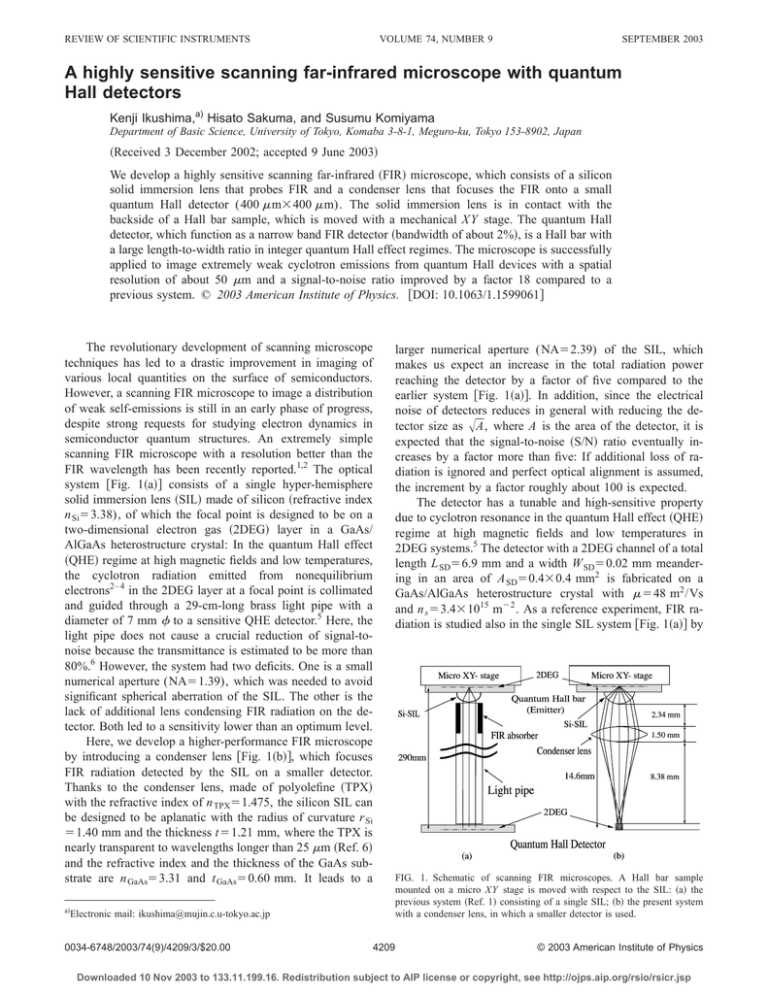
REVIEW OF SCIENTIFIC INSTRUMENTS VOLUME 74, NUMBER 9 SEPTEMBER 2003 A highly sensitive scanning far-infrared microscope with quantum Hall detectors Kenji Ikushima,a) Hisato Sakuma, and Susumu Komiyama Department of Basic Science, University of Tokyo, Komaba 3-8-1, Meguro-ku, Tokyo 153-8902, Japan 共Received 3 December 2002; accepted 9 June 2003兲 We develop a highly sensitive scanning far-infrared 共FIR兲 microscope, which consists of a silicon solid immersion lens that probes FIR and a condenser lens that focuses the FIR onto a small quantum Hall detector (400 m⫻400 m). The solid immersion lens is in contact with the backside of a Hall bar sample, which is moved with a mechanical XY stage. The quantum Hall detector, which function as a narrow band FIR detector 共bandwidth of about 2%兲, is a Hall bar with a large length-to-width ratio in integer quantum Hall effect regimes. The microscope is successfully applied to image extremely weak cyclotron emissions from quantum Hall devices with a spatial resolution of about 50 m and a signal-to-noise ratio improved by a factor 18 compared to a previous system. © 2003 American Institute of Physics. 关DOI: 10.1063/1.1599061兴 The revolutionary development of scanning microscope techniques has led to a drastic improvement in imaging of various local quantities on the surface of semiconductors. However, a scanning FIR microscope to image a distribution of weak self-emissions is still in an early phase of progress, despite strong requests for studying electron dynamics in semiconductor quantum structures. An extremely simple scanning FIR microscope with a resolution better than the FIR wavelength has been recently reported.1,2 The optical system 关Fig. 1共a兲兴 consists of a single hyper-hemisphere solid immersion lens 共SIL兲 made of silicon 共refractive index n Si⫽3.38), of which the focal point is designed to be on a two-dimensional electron gas 共2DEG兲 layer in a GaAs/ AlGaAs heterostructure crystal: In the quantum Hall effect 共QHE兲 regime at high magnetic fields and low temperatures, the cyclotron radiation emitted from nonequilibrium electrons2– 4 in the 2DEG layer at a focal point is collimated and guided through a 29-cm-long brass light pipe with a diameter of 7 mm to a sensitive QHE detector.5 Here, the light pipe does not cause a crucial reduction of signal-tonoise because the transmittance is estimated to be more than 80%.6 However, the system had two deficits. One is a small numerical aperture (NA⫽1.39), which was needed to avoid significant spherical aberration of the SIL. The other is the lack of additional lens condensing FIR radiation on the detector. Both led to a sensitivity lower than an optimum level. Here, we develop a higher-performance FIR microscope by introducing a condenser lens 关Fig. 1共b兲兴, which focuses FIR radiation detected by the SIL on a smaller detector. Thanks to the condenser lens, made of polyolefine 共TPX兲 with the refractive index of n TPX⫽1.475, the silicon SIL can be designed to be aplanatic with the radius of curvature r Si ⫽1.40 mm and the thickness t⫽1.21 mm, where the TPX is nearly transparent to wavelengths longer than 25 m 共Ref. 6兲 and the refractive index and the thickness of the GaAs substrate are n GaAs⫽3.31 and t GaAs⫽0.60 mm. It leads to a larger numerical aperture (NA⫽2.39) of the SIL, which makes us expect an increase in the total radiation power reaching the detector by a factor of five compared to the earlier system 关Fig. 1共a兲兴. In addition, since the electrical noise of detectors reduces in general with reducing the detector size as 冑A, where A is the area of the detector, it is expected that the signal-to-noise 共S/N兲 ratio eventually increases by a factor more than five: If additional loss of radiation is ignored and perfect optical alignment is assumed, the increment by a factor roughly about 100 is expected. The detector has a tunable and high-sensitive property due to cyclotron resonance in the quantum Hall effect 共QHE兲 regime at high magnetic fields and low temperatures in 2DEG systems.5 The detector with a 2DEG channel of a total length L SD⫽6.9 mm and a width W SD⫽0.02 mm meandering in an area of A SD⫽0.4⫻0.4 mm2 is fabricated on a GaAs/AlGaAs heterostructure crystal with ⫽48 m2 /Vs and n s ⫽3.4⫻1015 m⫺2 . As a reference experiment, FIR radiation is studied also in the single SIL system 关Fig. 1共a兲兴 by FIG. 1. Schematic of scanning FIR microscopes. A Hall bar sample mounted on a micro XY stage is moved with respect to the SIL: 共a兲 the previous system 共Ref. 1兲 consisting of a single SIL; 共b兲 the present system with a condenser lens, in which a smaller detector is used. a兲 Electronic mail: ikushima@mujin.c.u-tokyo.ac.jp 0034-6748/2003/74(9)/4209/3/$20.00 4209 © 2003 American Institute of Physics Downloaded 10 Nov 2003 to 133.11.199.16. Redistribution subject to AIP license or copyright, see http://ojps.aip.org/rsio/rsicr.jsp 4210 Rev. Sci. Instrum., Vol. 74, No. 9, September 2003 Ikushima, Sakuma, and Komiyama FIG. 4. Detector signal, scanned near the drain terminal as seen in the lower part of Fig. 2, at I emit⫽70 A. The spatial resolution is evaluated to be about 50 m. FIG. 2. 共Color兲 Image of the FIR microscope in Fig. 1共b兲. A Si-SIL on the top of a lens holder supporting a condenser lens and a small quantum Hall detector is in contact with the backside of a Hall bar sample by a BeCu spring. using a larger detector (L LD⫽168 mm and W LD⫽0.05 mm in an area of A LD⫽3.1⫻3.8 mm2 ), fabricated on the same GaAs/AlGaAs crystal. The emitter is a rectangular Hall bar (1⫻3 mm2 ) fabricated on a different GaAs/AlGaAs heterostructure crystal with the electron mobility ⫽38 m2 /Vs and the density n s ⫽3.2⫻1015 m⫺2 . Throughout the measurements, rectangular-wave currents, I emit , at 40 Hz are passed through two terminals in the Hall bar sample. Detector signals are recorded by means of a standard lock-in technique. The micro-XY stage, mechanically driven by stepper motors, can be controlled by a personal computer. As shown in Fig. 2, the Si-SIL on the top of a lens holder supporting the condenser lens and the small quantum Hall detector is in contact with the backside of a Hall bar sample by a BeCu spring. The optical system in Fig. 2, including the Hall bar sample as an emitter and the detector, is placed at the center of a superconducting magnet in a liquid helium cryostat. The FIG. 3. Comparison of V sig between the previous and present system. The time constant is fixed in the lock-in measurements. The lower schematic represents the line along which the probed point is scanned. length- and width-wise directions of the Hall bar sample are defined as the X and Y axis, respectively, as shown in the lower schematic of Fig. 3. Figure 3 shows the detector signals, V sig , obtained when the sample is scanned along the width-wise direction of the Hall bar as illustrated in the lower part of Fig. 3. Here, the Hall bar sample is in the QHE state of the filling factor ⫽2 at the current I emit⫽300 A at 7.71 T 共the wavelength of 93 m兲. It is evident that the S/N ratio is significantly improved in the present system 共solid line兲 compared to the single SIL system 共dotted line兲. The amplitude of the detecSD , in the present system increases by a factor tor signal, V sig SD , is reduced by a factor 5.6, 3.3 while the noise voltage, V noise yielding the improvement of the S/N ratio by a factor of 18. Enhancement of signal voltage, however, is far from the ideal although the noise voltage is reasonably reduced. The discrepancy might be ascribed to an ambiguity of refractive indexes of Si, GaAs, and TPX at low temperatures 共4.2 K兲 and in the FIR regions as well as to the loss on the condenser lens and slight misalignment of the optical system. Despite all of these the improvement is significant, demonstrating distinct advantage of the present optical system. The measurement at a smaller current, I emit⫽70 A, is also carried out to estimate the spatial resolution of this microscope 共Fig. 4兲. Assuming that the FIR radiation is emitted just on an FIG. 5. 共Color兲 Image of cyclotron emissions from the QHE Hall bar of ⫽2 at I emit⫽100 A. The bright regions at the corners near terminals indicate significant distribution of cyclotron emissions. The white rectangle marks the Hall bar sample. Downloaded 10 Nov 2003 to 133.11.199.16. Redistribution subject to AIP license or copyright, see http://ojps.aip.org/rsio/rsicr.jsp Rev. Sci. Instrum., Vol. 74, No. 9, September 2003 extremely small spot near the drain terminal,1 the resolution is derived from the full width of half maximum to be about 50 m, which is better than the one achieved by the single SIL system. The resolution here is supposed to be determined by the whole optical system rather than by the value of NA of the SIL alone. Figure 5 displays a high-resolution image of the cyclotron radiation due to nonequilibrium electrons generated in the QHE Hall bar, obtained by scanning the whole area of the Hall bar. Bright two regions at the diagonally opposite corners near terminals indicate the significant generation of nonequilibrium electrons at these corners. Spread of the spot near the source terminal suggests nonequilibrium electrons due to local breakdown of the quantum Hall state.7 These results prove the usefulness of this optical scheme for studying detailed distributions of nonequilibrium electrons in quantum Hall devices. In conclusion, we succeeded in enhancement of sensitivity by a factor of 18 as well as achievement of higher resolution on FIR microscope. This is enabled to detect much weaker cyclotron radiation than that at hot spots, and we can expect to obtain further information on the dynamics of nonequilibrium electrons in quantum Hall devices. Although this microscope has a disadvantage on spectroscopic studies ow- Notes 4211 ing to tunability limitation 共inflexibility of electron density兲 on QHE detector, this maybe overcome by combining illumination and a negative bias voltage for backside of the detector.5 This work is supported by a Grant-in-Aid for Specially Promoted Research from the Japanese Ministry of Education, Culture, Sports, Science and Technology, and by Solution Oriented Research for Science and Technology 共SORST兲, Japan Science and Technology Corporation 共JST兲. 1 Y. Kawano and S. Komiyama, Proceedings of the 25th International Conference Physics Semiconductors, Osaka, 2000, p. 921. 2 Y. Kawano, Y. Hisanaga, and S. Komiyama, Phys. Rev. B 59, 12537 共1999兲. 3 K. von Klitzing, G. Ebert, N. Kleinmichel, H. Obloh, G. Dorda, and G. Weimann, in Proceedings of the 17th International Conference on the Physics of Semiconductors, edited by J. D. Chadi and W. A. Harrison 共Springer, New York, 1985兲, p. 271. 4 N. N. Zinov’ev, A. V. Akimov, L. J. Challis, A. F. Jezierski, and M. Henini, Semicond. Sci. Technol. 9, 831 共1994兲. 5 Y. Kawano, Y. Hisanaga, H. Takenouchi, and S. Komiyama, J. Appl. Phys. 89, 4037 共2001兲. 6 L. C. Robinson, Methods of Experimental Physics 共Academic, New York, 1973兲, Vol. 10, p. 101. 7 Y. Kawano and S. Komiyama, Phys. Rev. B 61, 2931 共2000兲. Downloaded 10 Nov 2003 to 133.11.199.16. Redistribution subject to AIP license or copyright, see http://ojps.aip.org/rsio/rsicr.jsp

