ISL29101
Data Sheet
November 5, 2012
Features
Small, Low Power, Voltage-Output
Ambient Light Photo Detect IC
• 0.5 lux to 10,000 lux range
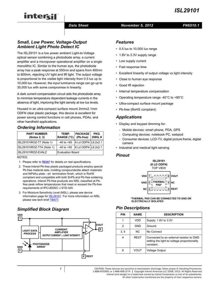
The ISL29101 is a low power ambient Light-to-Voltage
optical sensor combining a photodiode array, a current
amplifier and a micropower operational amplifier on a single
monolithic IC. Similar to the human eye, the photodiode
array has a peak response at 550nm and spans from 400nm
to 600nm, rejecting UV light and IR light. The output voltage
is proportional to the visible light intensity from 0.5 lux up to
10,000 lux. However, the input luminance range can go up to
30,000 lux with some compromise in linearity.
A dark current compensation circuit aids the photodiode array
to minimize temperature dependent leakage currents in the
absence of light, improving the light sensity at low lux levels.
Housed in an ultra-compact surface mount 2mmx2.1mm
ODFN clear plastic package, this device is excellent for
power saving control functions in cell phones, PDAs, and
other handheld applications.
• Low supply current
• Fast response time
• Excellent linearity of output voltage vs light intensity
• Close to human eye response
• Good IR rejection
• Internal temperature compensation
• Operating temperature range -40°C to +85°C
• Ultra-compact surface mount package
Applications
• Display and keypad dimming for:
TEMP.
PACKAGE PKG.
RANGE (°C) (Pb-free) DWG. #
ISL29101IROZ-T7 (Note 1)
-40 to +85
6 Ld ODFN L6.2x2.1
ISL29101IROZ-T7A (Note 1)
-40 to +85
6 Ld ODFN L6.2x2.1
ISL29101IROZ-EVALZ
• 1.8V to 3.3V supply range
• Pb-free (RoHS compliant)
Ordering Information
PART NUMBER
(Notes 2, 3)
Evaluation Board
- Mobile devices: smart phone, PDA, GPS
- Computing devices: notebook PC, webpod
- Consumer devices: LCD-TV, digital picture frame, digital
camera
• Industrial and medical light sensing
Pinout
NOTES:
ISL29101
(6 LD ODFN)
TOP VIEW
1. Please refer to TB347 for details on reel specifications.
2. These Intersil Pb-free plastic packaged products employ special
Pb-free material sets; molding compounds/die attach materials
and NiPdAu plate - e4 termination finish, which is RoHS
compliant and compatible with both SnPb and Pb-free soldering
operations. Intersil Pb-free products are MSL classified at Pbfree peak reflow temperatures that meet or exceed the Pb-free
requirements of IPC/JEDEC J STD-020.
VDD 1
GND 2
VDD
1
VOUT
GND
2
THERMAL
PAD*
5 NC
4 REXT
*THERMAL PAD CAN BE CONNECTED TO GND OR
ELECTRICALLY ISOLATED
Pin Descriptions
Simplified Block Diagram
LIGHT DATA
PROCESS
6 VOUT
NC 3
3. For Moisture Sensitivity Level (MSL), please see device
information page for ISL29101. For more information on MSL
please see tech brief TB477.
CURRENT
AMPLIFIER
OUTPUT CURRENT α LIGHT INTENSITY
FN6510.1
+
PIN
NAME
DESCRIPTION
1
VDD
Supply. 1.8V to 3.3V
2
GND
Ground
3, 5
NC
4
REXT
Connected to an external resistor to GND
setting the light-to-voltage proportionality
constant.
6
VOUT
Voltage Output
6
PHOTODIODE
ARRAY
No Connect
4 REXT
1
CAUTION: These devices are sensitive to electrostatic discharge; follow proper IC Handling Procedures.
1-888-INTERSIL or 1-888-468-3774 | Copyright Intersil Americas LLC 2008, 2012. All Rights Reserved
Intersil (and design) is a trademark owned by Intersil Corporation or one of its subsidiaries.
All other trademarks mentioned are the property of their respective owners.
ISL29101
Absolute Maximum Ratings (TA = +25°C)
Thermal Information
Supply Voltage between VDD and GND . . . . . . . . . . . . . . . . . . 3.6V
REXT . . . . . . . . . . . . . . . . . . . . . . . . . (-0.5V - GND) to (0.5V + VDD)
VOUT . . . . . . . . . . . . . . . . . . . . . . . . . (-0.5V - GND) to (0.5V + VDD)
VOUT Short Circuit Current . . . . . . . . . . . . . . . . . . . . . . . . . . <10mA
ESD Rating
Human Body Model . . . . . . . . . . . . . . . . . . . . . . . . . . . . . . .3000V
Machine Model . . . . . . . . . . . . . . . . . . . . . . . . . . . . . . . . . . . .300V
Thermal Resistance
θJA (°C/W)
6 Ld ODFN (Note 4) . . . . . . . . . . . . . . . . . . . . . . . . .
88
Maximum Die Temperature . . . . . . . . . . . . . . . . . . . . . . . . . . . +90°C
Storage Temperature . . . . . . . . . . . . . . . . . . . . . . . .-40°C to +100°C
Operating Temperature . . . . . . . . . . . . . . . . . . . . . . .-40°C to +85°C
Pb-Free Reflow Profile. . . . . . . . . . . . . . . . . . . . . . . . .see link below
http://www.intersil.com/pbfree/Pb-FreeReflow.asp
CAUTION: Do not operate at or near the maximum ratings listed for extended periods of time. Exposure to such conditions may adversely impact product
reliability and result in failures not covered by warranty.
NOTE:
4. θJA is measured in free air with the component mounted on a high effective thermal conductivity test board with “direct attach” features. See
Tech Brief TB379.
IMPORTANT NOTE: All parameters having Min/Max specifications are guaranteed. Typical values are for information purposes only. Unless otherwise noted, all tests
are at the specified temperature and are pulsed tests, therefore: TJ = TC = TA
Electrical Specifications
VDD = 3V, TA = +25°C, REXT = 100kΩ, no load at VOUT, green LED light, unless otherwise specified.
PARAMETER
DESCRIPTION
E
Range of Input Light Intensity
VDD
Power Supply Range
IDD
Supply Current
CONDITION
MIN
(Note 6)
TYP
MAX
(Note 6)
0.5 to 10k
1.8
UNIT
lux
3.3
V
35
µA
E = 1000 lux
23
E = 100 lux
3.5
µA
E = 0 lux
0.65
µA
165
mV
VOUT0
Light-to-Voltage Accuracy
E = 100 lux
VOUT1
Light-to-Voltage Accuracy
E = 1000 lux
VDARK
Voltage Output in the Absence of Light
ΔVOUT
1.65
2.13
V
E = 0 lux, RL = 10MΩ
1
25
mV
Output Voltage Variation Over Three Light Sources:
Fluorescent, Incandescent and Halogen
E = 1000 lux
20
%
PSRR
Power Supply Rejection Ratio
E = 100 lux, VDD = 1.8V to
3.3V
2.5
mV/V
VO-MAX
Maximum Output Compliance Voltage at 95% of
Nominal Output
VDD - 0.7V
V
tR
ISRC and ISNK Rise Time (Note 5)
E = 300 lux from 0 lux
104
µs
E = 1000 lux from 0 lux
27
µs
E = 300 lux to 0 lux
562
µs
E = 1000 lux to 0 lux
233
µs
E = 300 lux from 0 lux
504
µs
E = 1000 lux from 0 lux
209
µs
30
µs
18
µs
tF
tD
tS
ISRC and ISNK Fall Time (Note 5)
ISRC and ISNK Delay Time for Rising Edge (Note 5)
1.15
ISRC and ISNK Delay Time for Falling Edge (Note 5) E = 300 lux to 0 lux
E = 1000 lux to 0 lux
ISC
Short Circuit Current of Op Amp
±11
mA
SR
Slew Rate of Op Amp
±10
V/ms
VOS
Offset Voltage of Op Amp
±1.2
mV
NOTE:
5. Switching time measurement is based on Figures 1 and 2.
6. Compliance to datasheet limits is assured by one or more methods: production test, characterization and/or design.
2
FN6510.1
November 5, 2012
ISL29101
POWER SUPPLY
OR
SOURCE METER
INPUT
LIGHT
VDD
10%
90%
tr
ISL29101
FUNCTION
GENERATOR
tS
VOUT
tf%
90%
10%
OUTPUT
REXT
tD
FIGURE 2. TIMING DIAGRAM
FIGURE 1. TEST CIRCUIT FOR RISE/FALL TIME
MEASUREMENT
Typical Performance Curves
1.2
1.2
NORMALIZED LIGHT INTENSITY
HUMAN EYE RESPONSE
NORMALIZED RESPONSE
1.0
0.8
0.6
LIGHT SENSOR RESPONSE
0.4
0.2
0.0
-0.2
300
400
600
800
1.0k
FLUORESCENT
INCANDESCENT
1.0
0.8
SUN
HALOGEN
0.6
0.4
WLED
0.2
0
300
1.1k
400
500
WAVELENGTH (nm)
FIGURE 3. SPECTRAL RESPONSE
2.0
10°
0°
10°
20°
30°
40°
50°
50°
60°
60°
70°
70°
80°
80°
90°
90°
1.0
0.2 0.4
0.6 0.8
RELATIVE SENSITIVITY
FIGURE 5. RADIATION PATTERN
3
1000
1100
VDD = 3V
REXT = 10kΩ
1.8
OUTPUT VOLTAGE (V)
20°
900
FIGURE 4. SPECTRUM OF LIGHT SOURCES
RADIATION PATTERN
LUMINOSITY
30°
ANGLE 40°
600
700
800
WAVELENGTH (nm)
1.6
1.4
1.2
HALOGEN
1.0
INCANDESCENT
0.8
FLUORESCENT
0.6
0.4
0.2
0
0
1000 2000 3000 4000 5000 6000 7000 8000 9000 10000
LIGHT INTENSITY (LUX)
FIGURE 6. OUTPUT VOLTAGE vs LIGHT SENSITIVITY
FN6510.1
November 5, 2012
ISL29101
2.0
2.0
VDD = 3V
REXT = 100kΩ
1.8
1.6
1.4
1.2
HALOGEN
1.0
INCANDESCENT
0.8
FLUORESCENT
0.6
0.4
1.6
1.4
1.2
1.0
0.8
0.4
0.2
0
0
10
20
30 40 50 60 70
LIGHT INTENSITY (LUX)
80
90
18
16
OUTPUT VOLTAGE (mV)
FALL TIME
10.00
DELAY TIME BEFORE
BEFORE RISING
1.00
DELAY TIME BEFORE FALLING
0.10
14
12
10
RISE TIME
10
100
LUX CHANGE FROM 0 LUX (LUX)
1k
FIGURE 9. TRANSIENT TIME vs LUX CHANGE FROM 0 LUX
0.117
VDD = 3V
REXT = 10MΩ
LIGHT INTENSITY = 0 LUX
0.065
6
0.039
4
0.026
2
0.013
0
0
-0.013
-50 -40 -30 -20 -10 0 10 20 30 40 50 60 70 80 90 100
TEMPERATURE (°C)
FIGURE 10. OUTPUT VOLTAGE vs TEMPERATURE AT 0 LUX
1.02
NORMALIZED OUTPUT
VOLTAGE VARIATION
1.03
0.6
0.078
0.052
VDD = 3V
REXT = 10MΩ
1.2 LIGHT INTENSITY = 0 LUX
NO LOAD
0.8
0.091
VDD = 3V
REXT = 10MΩ
1.4
1.0
0.104
8
-2
0.01
1
100
FIGURE 8. OUTPUT VOLTAGE vs LIGHT INTENSITY
100.00
TRANSIENT TIME (ms)
INCANDESCENT
0
100 200 300 400 500 600 700 800 900 1000
LIGHT INTENSITY (LUX)
FIGURE 7. OUTPUT VOLTAGE vs LIGHT SENSITIVITY
SUPPLY CURRENT (µA)
FLUORESCENT
HALOGEN
0.6
0.2
0
VDD = 3V
REXT = 1MΩ
1.8
OUTPUT VOLTAGE (V)
OUTPUT VOLTAGE (V)
(Continued)
EQUIVALENT LIGHT INTENSITY (LUX)
Typical Performance Curves
VDD = 3V
FLUORESCENT LIGHT
1.01
1.00
300 LUX
0.99
1000 LUX
0.98
0.4
-50 -40 -30 -20 -10 0
10 20 30 40 50 60 70 80 90 100
TEMPERATURE (°C)
FIGURE 11. SUPPLY CURRENT vs TEMPERATURE AT 0 LUX
4
0.97
-50 -40 -30 -20 -10 0 10 20 30 40 50 60 70 80 90 100
TEMPERATURE (°C)
FIGURE 12. NORMALIZED OUTPUT VOLTAGE vs
TEMPERATURE
FN6510.1
November 5, 2012
ISL29101
Typical Performance Curves
(Continued)
1.02
SUPPLY CURRENT (µA)
20
18
1100 LUX
16
14
12
10
300 LUX
8
6
NO LOAD
4 VDD = 3V
REXT = 100kΩ
FLUORESCENT LIGHT
0
-50 -40 -30 -20 -10 0 10 20 30 40 50 60 70 80 90 100
NORMALIZED OUTPUT VOLTAGE
22
1.01
FLUORESCENT LIGHT INTENSITY = 1100 LUX
REXT = 100kΩ
VDD = 3
1.00
0.99
0.98
0.97
1.5
TEMPERATURE (°C)
2.5
3.0
3.5
4.0
SUPPLY VOLTAGE (V)
FIGURE 13. SUPPLY CURRENT vs TEMPERATURE
FIGURE 14. NORMALIZED OUTPUT VOLTAGE vs SUPPLY
VOLTAGE
23.0
LIGHT INTENSITY
FLUORESCENT LIGHT INTENSITY = 1100 LUX
LOAD
22.5 NO
VDD = 3
SUPPLY CURRENT
2.0
VDD = 3V, REXT = 100k:
LIGHT INTENSITY RISES FROM 0 LUX TO 300 LUX
AND FALLS FROM 300 LUX TO 0 LUX WITH
WHITE LED
22.0
21.5
21.0
VOUT
0V
20.5
20.0
1.5
2.0
2.5
3.0
SUPPLY VOLTAGE (V)
3.5
4.0
FIGURE 15. SUPPLY CURRENT vs SUPPLY VOLTAGE
5
FIGURE 16. TRANSIENT RESPONSE OF ISL29101 TO
CHANGE IN LIGHT INTENSITY
FN6510.1
November 5, 2012
ISL29101
Application Information
the ISL29101’s output circuit may result in premature
saturation when an excessively large REXT is used. The
output compliance voltage is 700mV below the supply
voltage, as listed in VO-MAX of the “Electrical Specifications”
table on page 2.
Light-to-Voltage Conversion
The ISL29101 has responsiveness that is a linear function of
the light intensity intercepted by the photodiode in lux.
Because the photodiode has a responsivity that resembles
the human eye, conversion rate is independent of the light
source (fluorescent light, incandescent light or direct
sunlight).
V OUT = ( 1.6μA ⁄ 100lux ) • E • R EXT
Optical Sensor Location Outline
The green area in Figure 17 shows the optical sensor
location outline of ISL29101. Along the pinout direction, the
center line (CL) of the sensor coincides with that of the
packaging. The sensor width in this direction is 0.39mm.
Perpendicular to the pin-out direction, the CL of the sensor
has an 0.19mm offset from the CL of packaging away from
pin-1. The sensor width in this direction is 0.46mm.
(EQ. 1)
Here, VOUT is the output voltage and E is the light intensity.
REXT is the value of the external resistor, which is used to
set the light-to-voltage scaling constant. The compliance of
2.10mm
2.00mm
SENSOR OFFSET
29101
0.46mm
0.19mm
0.39mm
FIGURE 17. 6 LD ODFN SENSOR LOCATION OUTLINE
All Intersil U.S. products are manufactured, assembled and tested utilizing ISO9000 quality systems.
Intersil Corporation’s quality certifications can be viewed at www.intersil.com/design/quality
Intersil products are sold by description only. Intersil Corporation reserves the right to make changes in circuit design, software and/or specifications at any time without
notice. Accordingly, the reader is cautioned to verify that data sheets are current before placing orders. Information furnished by Intersil is believed to be accurate and
reliable. However, no responsibility is assumed by Intersil or its subsidiaries for its use; nor for any infringements of patents or other rights of third parties which may result
from its use. No license is granted by implication or otherwise under any patent or patent rights of Intersil or its subsidiaries.
For information regarding Intersil Corporation and its products, see www.intersil.com
6
FN6510.1
November 5, 2012
ISL29101
Package Outline Drawing
L6.2x2.1
6 LEAD OPTICAL DUAL FLAT NO-LEAD PLASTIC PACKAGE (ODFN)
Rev 3, 5/11
2.10
A
6
PIN #1
INDEX AREA
B
6
PIN 1
INDEX AREA
1
0.65
1.35
2.00
1.30 REF
4 6X 0.30±0.05
(4X)
0.10
0.10 M C A B
0.65
TOP VIEW
6x0.35 ± 0.05
BOTTOM VIEW
2.50
PACKAGE
OUTLINE
2.10
SEE DETAIL "X"
0.65
(4x0.65)
0.10 C
MAX 0.75
C
BASE PLANE
SEATING PLANE
0.08 C
SIDE VIEW
(1.35)
(6x0.30)
C
(6x0.20)
0 . 2 REF
5
0 . 00 MIN.
0 . 05 MAX.
(6x0.55)
TYPICAL RECOMMENDED LAND PATTERN
DETAIL "X"
NOTES:
1.
Dimensions are in millimeters.
Dimensions in ( ) for Reference Only.
2.
Dimensioning and tolerancing conform to ASME Y14.5m-1994.
3.
Unless otherwise specified, tolerance : Decimal ± 0.05
4.
Dimension applies to the metallized terminal and is measured
between 0.15mm and 0.30mm from the terminal tip.
5.
Tiebar shown (if present) is a non-functional feature.
6.
The configuration of the pin #1 identifier is optional, but must be
located within the zone indicated. The pin #1 identifier may be
either a mold or mark feature.
7
FN6510.1
November 5, 2012
