HT78xx - Holtek
advertisement

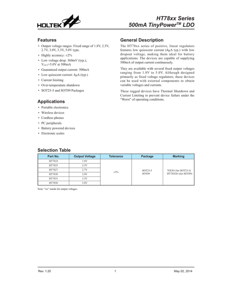
HT78xx Series 500mA TinyPowerTM LDO Features General Description • Output voltage ranges: Fixed range of 1.8V, 2.5V, 2.7V, 3.0V, 3.3V, 5.0V type. The HT78xx series of positive, linear regulators features low quiescent current (4mA typ.) with low dropout voltage, making them ideal for battery applications. The devices are capable of supplying 500mA of output current continuously. • Highly accuracy: ±2% • Low voltage drop: 360mV (typ.), VOUT=5.0V at 500mA They are available with several fixed output voltages ranging from 1.8V to 5.0V. Although designed primarily as fixed voltage regulators, these devices can be used with external components to obtain variable voltages and currents. • Guaranteed output current: 500mA • Low quiescent current: 4mA (typ.) • Current limiting • Over-temperature shutdown • SOT23-5 and SOT89 Packages These rugged devices have Thermal Shutdown and Current Limiting to prevent device failure under the "Worst" of operating conditions. Applications • Portable electronics • Wireless devices • Cordless phones • PC peripherals • Battery powered devices • Electronic scales Selection Table Part No. Output Voltage HT7818 1.8V HT7825 2.5V HT7827 2.7V HT7830 3.0V HT7833 3.3V HT7850 5.0V Tolerance Package ±2% SOT23-5 SOT89 Marking 78XX# (for SOT23-5) HT78XX# (for SOT89) Note: ″xx″ stands for output voltages. Rev. 1.20 1 May 02, 2014 HT78xx Block Diagram Pin Assignment Pin Description Pin No. Pin Name Description SOT23-5 SOT89 3 — CE 5 3 VOUT 1 2 VIN Input pin 2 1 GND Ground pin 4 — NC Rev. 1.20 Chip enable pin, high enable Output pin No connection 2 May 02, 2014 HT78xx Absolute Maximum Ratings* Storage Temperature............................−50°C to 125°C Maximum Supply Voltage...........................Up to 8.5V Operating Temperature..........................−40°C to 85°C Note: These are stress ratings only. Stresses exceeding the range specified under Absolute Maximum Ratings may cause substantial damage to the device. Functional operation of this device at other conditions beyond those listed in the specification is not implied and prolonged exposure to extreme conditions may affect device reliability. * Absolute maximum ratings indicate limits beyond which damage to the device may occur. Operating Ratings indicate conditions for which the device is intended to be functional, but do not guarantee specific performance limits. The guaranteed specifications apply only for the test conditions listed. Thermal Information Symbol θJA PD Parameter Thermal Resistance (Junction to Ambient) (Assume no ambient airflow, no heat sink) Power Dissipation Package Max. Unit SOT23-5 500 °C/W SOT89 200 °C/W SOT23-5 0.20 W SOT89 0.50 W Note: PD is measured at Ta= 25°C Electrical Characteristics Symbol Tj=25°C, VIN=VOUT+1.0V, IO=1mA, unless otherwise specified Parameter Test Conditions Min. Typ. Max. Unit VIN Input Voltage — — — 8 V ∆VOUT Output Voltage Tolerance — −2 — 2 % ISS Quiescent Current IO=0mA, VCE=VIN — 4 7 µA ∆VLOAD Load Regulation (Note1) 1mA ≤ IOUT ≤ 500mA — 0.004 0.008 %/mA — 800 1200 Dropout Voltage (Note2) ∆VOUT=2% IOUT=500mA VO ≤ 1.8V VDROP 2.5V ≤ VO ≤ 2.7V — 500 650 3.0V ≤ VO ≤ 5.0V — 360 500 ∆VLINE Line Regulation VOUT+1.0V≤VIN≤8.0V ILIM Current Limit (Note3) ∆VOUT=10% VIH CE Input High Threshold VIL ISD ∆VOUT ∆Ta mV — 0.2 0.3 %/V 500 — — mA VOUT + 1V ≤ VIN ≤ 8V 2 — — V CE Input Low Threshold VOUT + 1V ≤ VIN ≤ 8V — — 0.8 V Shutdown Current CE input voltage ≤ 0.8V — 0.5 1.0 µA Temperature Coefficient −40°C < Ta < 85°C — ±0.8 — mV/°C Note: 1. Load regulation is measured at a constant junction temperature, using pulse testing with a low ON time and is guaranteed up to the maximum power dissipation. Power dissipation is determined by the input/output differential voltage and the output current. Guaranteed maximum power dissipation will not be available over the full input/output range. The maximum allowable power dissipation at any ambient temperature is PD = (TJ(MAX) − Ta) / θJA. 2. Dropout voltage is defined as the input voltage minus the output voltage that produces a 2% change in the output voltage from the value at VIN = VOUT+1V with a fixed load. 3. Current limit is measured by pulsing for a short time. Rev. 1.20 3 May 02, 2014 HT78xx Application Circuit The circuits provided in this section are for reference only. For the purposes of clarity some of the detailed components pramaters shall depend on the application. Basic Circuits V V IN IN H L V V O U T S e r ie s C E C 1 1 F R2 R1 O U T C 2 2 .2 F G N D C o m m o n C o m m o n S in g le p o in t G N D Typical Application Circuits High Output Current Positive Voltage Regulator 4 Rev. 1.20 May 02, 2014 HT78xx Increased Output Voltage Circuit V V IN IN C 1 1 0 F IS C 2 1 0 F G N D S V V O U T S e r ie s V O U T R 1 X X R 2 C o m m o n S in g le p o in t G N D VOUT = VXX (1 + R2 R1 C o m m o n ) + ISS R2 Dual Supply Circuit IC 1 V V IN IN IC 2 C 1 1 0 F V G N D S e r ie s V IN V O U T S e r ie s X X 1 V C 3 1 0 F O U T 1 V O U T V C 2 1 0 F G N D C o m m o n R 1 V O U T 2 X X 2 C o m m o n S in g le p o in t G N D VOUT1 = VXX2 + VXX1 VOUT2 = VXX2 Tracking Voltage Regulator V V IN IN C 1 1 0 F V V O U T S e r ie s C 2 1 0 F G N D R A R B O U T S in g le p o in t G N D -V V IN -VO = VOUT × Rev. 1.20 5 O RB RA May 02, 2014 HT78xx Package Information Note that the package information provided here is for consultation purposes only. As this information may be updated at regular intervals users are reminded to consult the Holtek website for the latest version of the package information. Additional supplementary information with regard to packaging is listed below. Click on the relevant section to be transferred to the relevant website page. • Further Package Information (include Outline Dimensions, Product Tape and Reel Specifications) • Packing Meterials Information • Carton information Rev. 1.20 6 May 02, 2014 HT78xx 5-pin SOT23-5 Outline Dimensions Symbol Nom. Max. A 0.030 — 0.031 A1 0.000 — 0.002 A2 0.028 0.030 0.031 b 0.014 — 0.020 C 0.004 — 0.008 D — 0.114 BSC — E — 0.110 BSC — E1 — 0.063 BSC — e — 0.037 BSC — e1 — 0.075 BSC — L 0.015 0.018 0.024 L1 — 0.024 BSC — θ 0° — 8° Symbol Rev. 1.20 Dimensions in inch Min. Dimensions in mm Min. Nom. Max. A 0.75 — 0.80 A1 0.00 — 0.05 A2 0.70 0.75 0.78 b 0.35 — 0.50 C 0.10 — 0.20 D — 2.90 BSC — E — 2.80 BSC — E1 — 1.60 BSC — e — 0.95 BSC — e1 — 1.90 BSC — L 0.37 0.45 0.60 L1 — 0.60 BSC — θ 0° — 8° 7 May 02, 2014 HT78xx 3-pin SOT89 Outline Dimensions Symbol Dimensions in inch Min. Nom. Max. A 0.173 — 0.181 B 0.053 — 0.072 C 0.090 — 0.102 D 0.035 — 0.047 E 0.155 — 0.167 F 0.014 — 0.019 G 0.017 — 0.022 H — 0.059 BSC — I 0.055 — 0.063 J 0.014 — 0.017 Symbol Rev. 1.20 Dimensions in mm Min. Nom. Max. A 4.40 — 4.60 B 1.35 — 1.83 C 2.29 — 2.60 D 0.89 — 1.20 E 3.94 — 4.25 F 0.36 — 0.48 G 0.44 — 0.56 H — 1.50 BSC — I 1.40 — 1.60 J 0.35 — 0.44 8 May 02, 2014 HT78xx Copyright© 2014 by HOLTEK SEMICONDUCTOR INC. The information appearing in this Data Sheet is believed to be accurate at the time of publication. However, Holtek assumes no responsibility arising from the use of the specifications described. The applications mentioned herein are used solely for the purpose of illustration and Holtek makes no warranty or representation that such applications will be suitable without further modification, nor recommends the use of its products for application that may present a risk to human life due to malfunction or otherwise. Holtek's products are not authorized for use as critical components in life support devices or systems. Holtek reserves the right to alter its products without prior notification. For the most up-to-date information, please visit our web site at http://www.holtek.com.tw. Rev. 1.20 9 May 02, 2014


