HT77xxSA PFM DC/DC Step-up Converter
advertisement

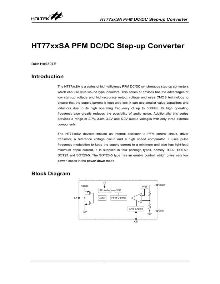
HT77xxSA PFM DC/DC Step-up Converter HT77xxSA PFM DC/DC Step-up Converter D/N: HA0307E Introduction The HT77xxSA is a series of high-efficiency PFM DC/DC synchronous step-up converters, which can use wire-wound type inductors. This series of devices has the advantages of low start-up voltage and high-accuracy output voltage and uses CMOS technology to ensure that the supply current is kept ultra-low. It can use smaller value capacitors and inductors due to its high operating frequency of up to 500kHz. Its high operating frequency also greatly reduces the possibility of audio noise. Additionally, this series provides a range of 2.7V, 3.0V, 3.3V and 5.0V output voltages with only three external components. The HT77xxSA devices include an internal oscillator, a PFM control circuit, driver transistor, a reference voltage circuit and a high speed comparator. It uses pulse frequency modulation to keep the supply current to a minimum and also has light-load minimum ripple current. It is supplied in four package types, namely TO92, SOT89, SOT23 and SOT23-5. The SOT23-5 type has an enable control, which gives very low power losses in the power-down mode. Block Diagram L X V O U T V re f L X L im ite r L X B u ffe r O S C P F M C o n tro l C h ip E n a b le C E 1 V O U T G N D HT77xxSA PFM DC/DC Step-up Converter Pin Assignment S O T 8 9 T O 9 2 V O U T 3 F r o n t V ie w 1 2 S O T 2 3 -5 S O T 2 3 L X 5 G N D 4 3 T o p V ie w T o p V ie w G N D V O U T L X B o tto m 1 2 3 G N D V O U T L X G N D V O U T L X 1 2 1 2 3 G N D L X C E V O U T N C G N D L X C E V O U T N C V ie w Pin Description Package Type Name TO92 SOT89 SOT23 SOT23-5 — — — 1 CE 2 2 3 2 VOUT — — — 3 NC 1 1 1 4 GND 3 3 2 5 LX Description Enable pin. When the pin is set high, the device is enabled and, when low, the device is disabled. Applicaion Circuit Application Circuit without CE Pin 2 Output line Reserved line Ground Switching signal line HT77xxSA PFM DC/DC Step-up Converter Application Circuit with CE Pin Functional Description The HT77xxSA is a series of synchronous step-up converter using pulse frequency modulation to control the time constant. The PFM control method is essentially stable, however the necessary inuput/output capacitors and inductors must be carefully selected to prevent instability. The HT77xxSA contains a fully integrated synchronous rectifier, thereby reducing costs. This is due to smaller inductors sizes, capacitors sizes and the elimination of the need for a schottky diode cost as well as smaller circuit board areas. The real load circuit ensures that the HT77xxSA is fully shut-down. Low-power Start The HT77xxSA has a very low start voltage of about 0.7V. When connected to the supply power, the initial synchronisation switch will be turned off, but the energy is transferred through the body diodes to the load. Shut-down Mode The EN line should be high for the normal operating mode or be connected to the VOUT line or the VIN power line. When the EN line is low the device enters the power-down mode and the internal circuits will be powered down. During the power-down mode, the PMOS power transistor is turned off and the output will be in a floating state. 3 HT77xxSA PFM DC/DC Step-up Converter Synchronous Rectification During the shut down operation, there is a dead time between the N-channel and P-channel Mosfet switching. The usual schottky diode is replaced by the P-channel Mosefet during synchronous rectification. At the same time, the P-channel must be turned off before the N-channel conducts. After one cycle, it requires a period of 30ns dead time to ensure that the N-channel is completely turned off before the P-channel conducts. In this way it can maintain high efficiency operation for a variety of input voltages and output power ranges. Application Information Inductor Selection Taking into account the output current requirements, the inductor saturation current and the acceptable voltage ripple, selecting a proper inductor is an important factor to consider. A smaller value inductor provides a higher output current, but results in a higher ripple voltage and reduced efficiency. A higher inductor value reduces the output ripple voltage and improves efficiency, but also limits the output current. For the inductor selection, lower core losses and lower DC impedances can provide higher efficiencies. The three important parameters, the inductance value, the DCR and the saturation current must be considered when selecting the inductors. The inductor peak current can be calculated by the following formula: I L ( PEAK ) VOUT I O V IN (VOUT V IN ) 2 VOUT L V IN In the above formula: VIN —— input voltage VOUT —— output voltage IO —— output current η —— efficiency L —— inductor value 4 HT77xxSA PFM DC/DC Step-up Converter Capacitor Selection The output capacitor selection will also affect operating efficiency and output ripple voltage, therefore it must be selected for maximum efficiency. The output ripple voltage is generated when the current is at its peak inductor current and is related to the ESR, which is the capacitor equivalent series resistance. Using a low ESR capacitor is a very important factor to achieve the desired operation. Paralleling a number of filter capacitors together will result in lower ESR values. This application example shows the HT77xxSA efficiency when using wire-wound and multi-layer capacitors. The Efficiency when Using Wire-wound Capacitor The Efficiency when Using Wire-wound Capacitor 100% 80% 80% Efficiency (%) Efficiency (%) HT7733SA 100% 60% 40% 60% 40% VIN=2.0V VIN=2.0V VIN=1.8V 20% VIN=1.8V 20% VIN=1.5V VIN=1.5V VIN=1.2V VIN=1.2V 0% 0% 0 50 100 150 200 250 0 50 Output Current (mA) 100 150 200 250 Output Current (mA) Fig 1. L use ABC SR0302 Fig 2. L use ABC SR0503 100% 100% 80% 80% Efficiency (%) Efficiency (%) HT7730SA 60% 40% 60% 40% VIN=2.0V VIN=2.0V VIN=1.8V 20% VIN=1.8V 20% VIN=1.5V VIN=1.5V VIN=1.2V VIN=1.2V 0% 0% 0 50 100 150 200 250 0 Output Current (mA) 50 100 150 200 Output Current (mA) Fig 3. L use ABC SR0302 Fig 4. L use ABC SR0503 5 250 HT77xxSA PFM DC/DC Step-up Converter Layout Considerations The circuit board layout is important for stable switching operation. Poor layout may lead to associated noise. In order to reduce both EMI and switching noise, note the follwing recommendations: Line width should be as wide as possible Input/output capacitors should be located as close as possible to the VIN, VOUT and GND pins Ground connections can help to prevent electromagnetic interfernce A recommended PCB layout and component location diagram is shown below: 6 HT77xxSA PFM DC/DC Step-up Converter Conclusion This article has explained in detail the HT77xxSA internal functional operation and functional description. It has also introduced HT77xxSA applications and discussed performance efficiency when using wire-wound inductors. Appendix Components List: Component Type Manufacturer CIN, COUT GJ831CR61E106KE83L Murata L SR03023100MLB ABC Taiwan Electronics Corp. L SR0503100MLB ABC Taiwan Electronics Corp. 7 Parameter 10μF, 25V. X5R ceramic capacitor. 10μH, RDC=0.25Ω. wire-wound power inductor 10μH, RDC=0.13Ω. wire-wound power inductor.


