Time-Resolved Detection of Single
advertisement
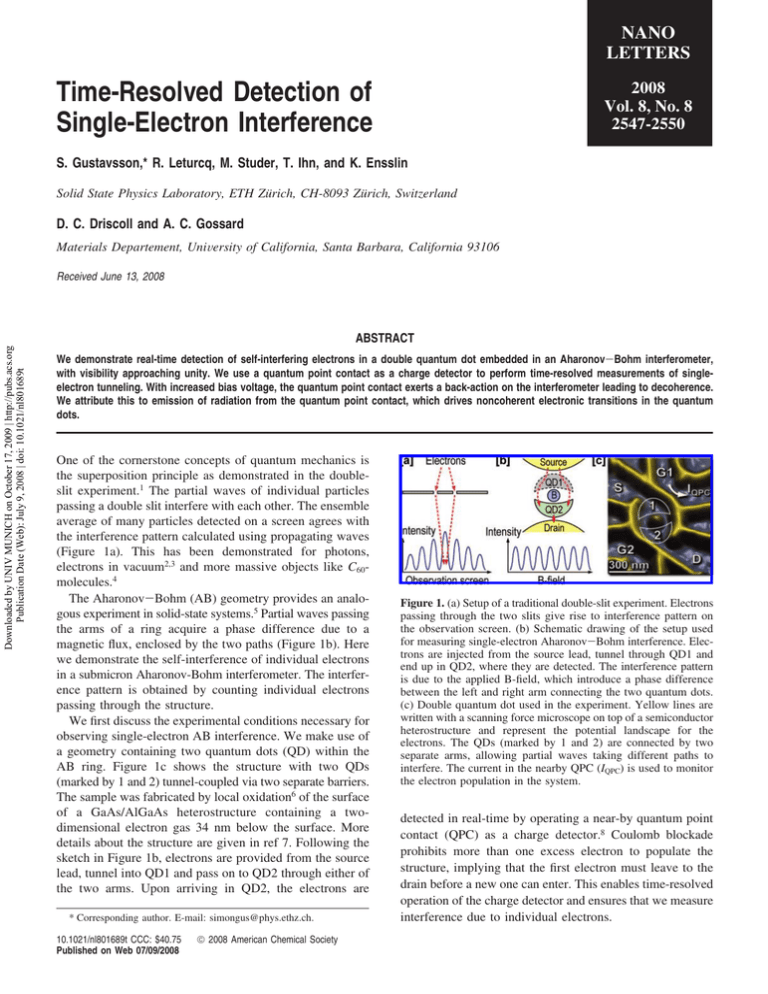
NANO LETTERS Time-Resolved Detection of Single-Electron Interference 2008 Vol. 8, No. 8 2547-2550 S. Gustavsson,* R. Leturcq, M. Studer, T. Ihn, and K. Ensslin Solid State Physics Laboratory, ETH Zürich, CH-8093 Zürich, Switzerland D. C. Driscoll and A. C. Gossard Materials Departement, UniVersity of California, Santa Barbara, California 93106 Received June 13, 2008 Downloaded by UNIV MUNICH on October 17, 2009 | http://pubs.acs.org Publication Date (Web): July 9, 2008 | doi: 10.1021/nl801689t ABSTRACT We demonstrate real-time detection of self-interfering electrons in a double quantum dot embedded in an Aharonov-Bohm interferometer, with visibility approaching unity. We use a quantum point contact as a charge detector to perform time-resolved measurements of singleelectron tunneling. With increased bias voltage, the quantum point contact exerts a back-action on the interferometer leading to decoherence. We attribute this to emission of radiation from the quantum point contact, which drives noncoherent electronic transitions in the quantum dots. One of the cornerstone concepts of quantum mechanics is the superposition principle as demonstrated in the doubleslit experiment.1 The partial waves of individual particles passing a double slit interfere with each other. The ensemble average of many particles detected on a screen agrees with the interference pattern calculated using propagating waves (Figure 1a). This has been demonstrated for photons, electrons in vacuum2,3 and more massive objects like C60molecules.4 The Aharonov-Bohm (AB) geometry provides an analogous experiment in solid-state systems.5 Partial waves passing the arms of a ring acquire a phase difference due to a magnetic flux, enclosed by the two paths (Figure 1b). Here we demonstrate the self-interference of individual electrons in a submicron Aharonov-Bohm interferometer. The interference pattern is obtained by counting individual electrons passing through the structure. We first discuss the experimental conditions necessary for observing single-electron AB interference. We make use of a geometry containing two quantum dots (QD) within the AB ring. Figure 1c shows the structure with two QDs (marked by 1 and 2) tunnel-coupled via two separate barriers. The sample was fabricated by local oxidation6 of the surface of a GaAs/AlGaAs heterostructure containing a twodimensional electron gas 34 nm below the surface. More details about the structure are given in ref 7. Following the sketch in Figure 1b, electrons are provided from the source lead, tunnel into QD1 and pass on to QD2 through either of the two arms. Upon arriving in QD2, the electrons are * Corresponding author. E-mail: simongus@phys.ethz.ch. 10.1021/nl801689t CCC: $40.75 Published on Web 07/09/2008 2008 American Chemical Society Figure 1. (a) Setup of a traditional double-slit experiment. Electrons passing through the two slits give rise to interference pattern on the observation screen. (b) Schematic drawing of the setup used for measuring single-electron Aharonov-Bohm interference. Electrons are injected from the source lead, tunnel through QD1 and end up in QD2, where they are detected. The interference pattern is due to the applied B-field, which introduce a phase difference between the left and right arm connecting the two quantum dots. (c) Double quantum dot used in the experiment. Yellow lines are written with a scanning force microscope on top of a semiconductor heterostructure and represent the potential landscape for the electrons. The QDs (marked by 1 and 2) are connected by two separate arms, allowing partial waves taking different paths to interfere. The current in the nearby QPC (IQPC) is used to monitor the electron population in the system. detected in real-time by operating a near-by quantum point contact (QPC) as a charge detector.8 Coulomb blockade prohibits more than one excess electron to populate the structure, implying that the first electron must leave to the drain before a new one can enter. This enables time-resolved operation of the charge detector and ensures that we measure interference due to individual electrons. Downloaded by UNIV MUNICH on October 17, 2009 | http://pubs.acs.org Publication Date (Web): July 9, 2008 | doi: 10.1021/nl801689t Figure 2. (a) Charge stability diagram of the double quantum dot, recorded by counting electrons entering and leaving the structure. The data were taken at bias voltage Vb ) 600 µV and B ) 0 T. (b) Tunneling rates for electrons entering (red) an leaving (blue) the DQD, measured along the dashed white line in (a). The upper x-axis shows δa, the potential difference between the state in QD2 and the occupied state of QD1. The solid lines are tunneling rates expected from sequential tunneling, and the dashed line is a fit to the cotunneling model of eq 1. Parameters are given in the text. The data was taken with B ) 340 mT. (c) Energy level configuration of the DQD at the point marked by II in (a, b). Electron transport from source to QD2 is possible by means of cotunneling. (d) Schematic drawing of the cotunneling process. (e) Number of electrons arriving at QD2 within the fixed period of time indicated in the upper-right corner, measured as a function of magnetic field. The data was taken at point II in (a). The count rate shows an oscillatory pattern with a visibility higher than 90%. To avoid dephasing, the electrons should spend a time as short as possible on their way from source to QD2. This is achieved by raising the electrochemical potential of QD1 so that electrons in the source lead lack an energy δ required for entering QD1 (see Figure 2c). The time-energy uncertainty principle still allows electrons to tunnel from source to QD2 by means of a second order process. The electron dwell time in QD1 is then limited to a short time scale set by the uncertainty relation, with t ) p/δ.9 The charge detector is implemented by tuning the QPC conductance close to 0.5 × 2e2/h. At this point the QPC conductance is highly sensitive to changes in its electrostatic surroundings, allowing it to be used to detect single electrons tunneling into or out of the QD in real time.10–12 The QPC conductance was measured by applying a dc bias voltage over the QPC, VQPC ) 250 µV, and monitoring the current IQPC. The charge detection technique allows the tunneling rates for electrons entering and leaving the double QD (DQD) to be determined separately.13,14 In the experiment, we apply appropriate gate voltages to tune the tunneling rates between the DQD and the source and drain leads to values below 15 kHz. The tunnel couplings between the QDs are set to a few GHz. The interdot 2548 transitions are too fast to be detected with the bandwidth of the charge detector (Γdet ) 20 kHz), but the coupling energy can still be determined from charge localization measurements.15 Figure 2a shows the charge stability diagram of the DQD, measured by counting electrons entering and leaving the structure within a fixed period of time. The data was taken with 600 µV bias applied between source and drain. The hexagon pattern together with the triangles of electron transport appearing due to the applied bias are well-known characteristics of DQD systems.16 Between the triangles, there are band-shaped regions with weak but nonzero count rates where electron tunneling is expected to be suppressed due to Coulomb blockade. The finite count rate in these regions can be attributed to electron tunneling involving virtual processes.17 To investigate these processes in more detail, we follow the lines of ref 17 and plot the rates for electrons tunneling into and out of the DQD measured along the dashed line in Figure 2a. The result is shown in Figure 2b. Going along the dashed line in Figure 2a corresponds to lowering the electrochemical potential of QD1 while keeping the potential of QD2 constant. In the region marked by I, electrons tunnel sequentially from the source into QD1, continue from QD1 to QD2 and finally leave QD2 to the drain lead. Proceeding to point II in Figure 2a,b, the electrochemical potential of QD1 is lowered and an electron is trapped in QD1 (see sketch in Figure 2c). The electron lacks an energy δa to leave to QD2, but because of time-energy uncertainty there is a timewindow of length ∼p/δa within which tunneling from QD1 to QD2 followed by tunneling from the source into QD1 is possible without violating energy conservation. An analogous process is possible involving the next unoccupied state of QD1, occurring on time scales ∼p/δb. The processes correspond to electron cotunneling from the source lead to QD2. By continuing to point III, the unoccupied state of QD1 is shifted into the bias window and electron transport is again sequential. The solid lines in Figure 2b show the tunneling rates expected from sequential tunneling.18 The fit gives the tunnel couplings between source and the occupied (ΓSa)/unoccupied (ΓSb) states of QD1, with ΓSa ) 6.4 kHz and ΓSb ) 14 kHz. In the cotunneling regions we fit the data to an expression involving the sum of the two cotunneling processes:9,17 Γcot ) ΓSata2/δa2 + ΓSbtb2/δb2 (1) Here, ta, tb are the tunnel couplings between the occupied/ unoccupied states in QD1 and the state in QD2. The values for ΓSa and ΓSb are taken from measurement in the sequential regimes. The dashed line in Figure 2b shows the results of eq 1, with fitting parameters ta ) 8.3 µeV and tb ) 13 µeV. These values are in good agreement with values obtained from the charge localization measurements. We emphasize that eq 1 is valid only if δa, δb . ta, tb and if sequential transport is sufficiently suppressed, i.e., in the range 46 mV < VG1 < 48.6 mV of Figure 2b. Coming back to the sketch of Figure 1b, we note that the cotunneling configuration of case II in Figure 2a-c is ideal for investigating the Aharonov-Bohm effect for single Nano Lett., Vol. 8, No. 8, 2008 Downloaded by UNIV MUNICH on October 17, 2009 | http://pubs.acs.org Publication Date (Web): July 9, 2008 | doi: 10.1021/nl801689t Figure 4. (a) Aharonov-Bohm (AB) oscillations measured at different temperatures. At ∼400 mK, the visibility of the oscillations drops drastically. The data were taken along the dashed line in (b). (b) Amplitude of AB oscillations measured at different QPC bias. The inset shows a few photon absorption processes that are possible at large QPC bias. Figure 3. (a) Tunneling rates for electrons entering (Γin) and leaving (Γout) the DQD, measured versus electrochemical potential of QD1 and magnetic field. The y-axis corresponds to sweeps along the dashed line in Figure 2a. Within the cotunneling region, Γin shows clear B-field periodicity, and Γout remains constant. This is in agreement with the picture where only the electrons tunneling from source to QD2 encircle the Aharonov-Bohm ring, and electrons leaving to drain remains unaffected by the applied B-field. (b) Same as (a), but with reverse bias over the DQD. Here, the roles of Γin and Γout are inverted. electrons. Due to the low probability of the cotunneling process, the source lead provides low-frequency injection of single electrons into the DQD. The injected electrons cotunnel through QD1 into QD2 on a time scale t ∼ p/δ ∼ 1 ps much shorter than typical decoherence times of the system.19 This ensures that phase coherence is preserved. Finally, the electron stays in QD2 for a time long enough to be registered by the finite-bandwidth charge detector. The tunneling processes are visualized in Figure 2d. To proceed, we tune the system to case II of Figure 2a,b and count electrons as a function of magnetic field. Figure 2e shows snapshots of the number of electrons arriving in QD2 after three different times. The electrons travel oneby-one through the system but still build up a wellpronounced interference pattern with period 130 mT. This corresponds well to one flux quantum Φ ) h/e penetrating the area enclosed by the two paths. The visibility of the AB oscillations is higher than 90%, which is a remarkably large number demonstrating the high degree of phase coherence in the system. We attribute the high visibility to the short time available for the cotunneling process20 and to strong suppression of electrons being backscattered in the reverse direction, which is otherwise present in AB experiments. Another requirement for the high visibility is that the two tunnel barriers connecting the QDs are carefully symmetrized. The overall decay of the maxima of the AB oscillation with increasing B is probably due to magnetic field effects on the orbital wave functions in QD1 and QD2. Figure 3a shows the separate rates for electrons tunneling into and out of the DQD as a function of magnetic field. The y-axis corresponds to the dashed line in Figure 2a, i.e., to the energy of the states in QD1. The measurement shows a general shift of the DQD energy with the applied B-field, Nano Lett., Vol. 8, No. 8, 2008 which we attribute to changes of the orbital wave functions in the individual QDs. Within the cotunneling region, Γin shows well-defined B-periodic oscillations. At the same time, Γout is essentially independent of the applied field. This is expected because Γout measures the rate at which electrons leave QD2 to the drain, which occurs independently of the magnetic flux passing through the AB ring (see Figure 2c,d). In Figure 3b, the bias over the DQD is reversed. This inverts the roles of Γin and Γout so that Γout corresponds to the cotunneling process. Consequently, Γout shows B-periodic oscillations and Γin remains unaffected. In the black regions seen in Figure 3b no counts were registered within the measurement time of 3 s due to strong destructive interference for the tunneling-out process. As a consequence, we could not determine the tunneling rates in those regions. In Figure 4a, we investigate how the AB oscillations are influenced by elevated temperatures. The dephasing of open QD systems is thought to be due to electron-electron interaction,21 giving dephasing rates that depend strongly on temperature.22 Figure 3a shows the temperature dependence of the AB oscillations in our system. The amplitude of the oscillations remains almost unaffected up to ∼400 mK, indicating that the coherence is not affected by temperature until the thermal energy becomes comparable to the singlelevel spacing of the QDs. We conclude that the decreased visibility at higher temperatures is due to an increase in thermal fluctuations of the QD population. Decoherence can also occur because of interactions with the environment. In the experiment, we use the current in the QPC to detect the charge distribution in the DQD. In principle, the QPC could also determine whether an electron passed through the left or the right arm of the ring, thus acting as a which-path detector.23,24 If the QPC were to detect the electron passing in one of the arms, the interference pattern should disappear. In Figure 4b, we show the visibility of the AB oscillations as a function of bias on the QPC. The visibility remains unaffected up to VQPC ∼ 250 µeV but drops for higher bias voltages. We argue that the reduced visibility is not due to whichpath detection. At VQPC ) 400 µV, the current through the QPC is approximately 10 nA. This gives an average time delay between two electrons passing the QPC of e/IQPC ∼ 16 ps. Becuase this is 10 times larger than the typical cotun2549 Downloaded by UNIV MUNICH on October 17, 2009 | http://pubs.acs.org Publication Date (Web): July 9, 2008 | doi: 10.1021/nl801689t neling time, it is unlikely that the electrons in the QPC are capable of performing an effective which-path measurement. Instead, we attribute the decrease of the AB visibility to processes where the DQD absorbs photons emitted from the QPC. Previous work has shown that such processes may indeed excite an electron from one QD to the other, as long as the energy difference between the QDs is lower than the energy provided by the QPC bias.7 The radiation of the QPC may also drive transitions within the individual QDs, thus putting one of the QDs into an excited state.25,26 A few absorption processes are sketched in the inset of Figure 4b. As long as the QPC bias is lower than both the DQD detuning (δ ) 400 µeV) and the single-level spacing of the individual QDs (∆E ∼ 200 µeV), the AB visibility in Figure 4b is close to unity. When raising the QPC bias above ∆E, we start exciting the individual QDs. With increased QPC bias, more states become available and the absorption process becomes more efficient. This introduces new virtual paths for the cotunneling process. Becuase the different paths may interfere destructively, the interference pattern is eventually washed out. In this way, the QPC has a physical back-action on the measurement which is different from informational back-action27 and which-path detection previously investigated.23,24 In summary, we have demonstrated interference of single electrons in a solid-state environment. Such experiments have so far been limited to photons or massive particles in a highvacuum environment to decouple the quantum mechanical degrees of freedom as much as possible from the environment. Our experiments demonstrate the exquisite control of modern semiconductor nanostructures which enables interference experiment at the level of single quasi-particles in a solid-state environment. Once extended to include spin degrees of freedom28 such experiments have the potential to facilitate entanglement detection29 or investigate the interference of particles30 originating from different sources. Supporting Information Available: Movie showing how the interference pattern is built up in real-time as electrons pass through the structure one-by-one. This material is available free of charge via the Internet at http://pubs.acs.org. References (1) Young, T. Philos. Trans. R. Soc. London, 1804, 94, 1. (2) Jönsson, C. Phys. Z. 1961, 161, 454. 2550 (3) Tonomura, A.; Endo, J.; Matsuda, T.; Kawasaki, T.; Ezawa, H. Am. J. Phys. 1989, 57, 117. (4) Arndt, M.; Nairz, O.; Vos-Andreae, J.; Keller, C.; van der Zouw, G.; Zeilinger, A. Nature 1999, 401, 680. (5) Aharonov, Y.; Bohm, D. Phys. ReV. 1959, 115, 485. (6) Fuhrer, A.; Dorn, A.; Lüscher, S.; Heinzel, T.; Ensslin, K.; Wegscheider, W.; Bichler, M. Superl. Microstruct. 2002, 31, 19. (7) Gustavsson, S.; Studer, M.; Leturcq, R.; Ihn, T.; Ensslin, K.; Driscoll, D. C.; Gossard, A. C. Phys. ReV. Lett. 2007, 99, 206804. (8) Field, M.; Smith, C. G.; Pepper, M.; Ritchie, D. A.; Frost, J. E. F.; Jones, G. A. C.; Hasko, D. G. Phys. ReV. Lett. 1993, 70, 1311. (9) Averin, D. V.; Nazarov, Y. V. Single Charge Tunneling; Plenum: New York, 1992. (10) Vandersypen, L. M. K.; Elzerman, J. M.; Schouten, R. N.; Willems van Beveren, L. H.; Hanson, R.; Kouwenhoven, L. P. Appl. Phys. Lett. 2004, 85, 4394. (11) Schleser, R.; Ruh, E.; Ihn, T.; Ensslin, K.; Driscoll, D. C.; Gossard, A. C. Appl. Phys. Lett. 2004, 85, 2005. (12) Fujisawa, T.; Hayashi, T.; Hirayama, Y.; Cheong, H. D.; Jeong, Y. H. Appl. Phys. Lett. 2004, 84, 2343. (13) Gustavsson, S.; Leturcq, R.; Simovic, B.; Schleser, R.; Ihn, T.; Studerus, P.; Ensslin, K.; Driscoll, D. C.; Gossard, A. C. Phys. ReV. Lett. 2006, 96, 076605. (14) Naaman, O.; Aumentado, J. Phys. ReV. Lett. 2006, 96, 100201. (15) DiCarlo, L.; Lynch, H. J.; Johnson, A. C.; Childress, L. I.; Crockett, K.; Marcus, C. M.; Hanson, M. P.; Gossard, A. C. Phys. ReV. Lett. 2004, 92, 226801. (16) van der Wiel, W. G.; De Franceschi, S.; Elzerman, J. M.; Fujisawa, T.; Tarucha, S.; Kouwenhoven, L. P. ReV. Mod. Phys. 2002, 75, 1. (17) Gustavsson, S.; Studer, M.; Leturcq, R.; Ihn, T.; Ensslin, K.; Driscoll, D. C.; Gossard, A. C. 2008, arXiv.org:0805.3395. (18) Kouwenhoven, L. P.; Marcus, C. M.; McEuen, S.; Tarucha, P. M.; Westervelt, R. M.; Wingreen, N. S. In Mesoscopic Electron Transport; Sohn, L. L., Kouwenhoven, L. P., Schön, G., Eds.; NATO ASI Ser. E 345; Kluwer: Dordrecht, The Netherlands, 1997; pp 105-214. (19) Eisenberg, E.; Held, K.; Altshuler, B. L. Phys. ReV. Lett. 2002, 88, 136801. (20) Sigrist, M.; Ihn, T.; Ensslin, K.; Loss, D.; Reinwald, M.; Wegscheider, W. Phys. ReV. Lett. 2006, 96, 036804. (21) Altshuler, B. L.; Gefen, Y.; Kamenev, A.; Levitov, L. S. Phys. ReV. Lett. 1997, 78, 2803. (22) Huibers, A. G.; Switkes, M.; Marcus, C. M.; Campman, K.; Gossard, A. C. Phys. ReV. Lett. 1998, 81, 200. (23) Buks, E.; Schuster, R.; Heiblum, M.; Mahalu, D.; Umansky, V. Nature 1998, 391, 871. (24) Neder, I.; Heiblum, M.; Mahalu, D.; Umansky, V. Phys. ReV. Lett. 2007, 98, 036803. (25) Onac, E.; Balestro, F.; van Beveren, L. H. W.; Hartmann, U.; Nazarov, Y. V.; Kouwenhoven, L. P. Phys. ReV. Lett. 2006, 96, 176601. (26) Gustavsson, S.; Shorubalko, I.; Leturcq, R.; Ihn, T.; Ensslin, K.; Schon, S. 2008, arXiv.org:0805.1341. (27) Sukhorukov, E. V.; Jordan, A. N.; Gustavsson, S.; Leturcq, R.; Ihn, T.; Ensslin, K. Nature Phys. 2007, 3, 243. (28) Loss, D.; Sukhorukov, E. V. Phys. ReV. Lett. 2000, 84, 1035. (29) Saraga, D. S.; Loss, D. Phys. ReV. Lett. 2003, 90, 166803. (30) Neder, I.; Ofek, N.; Chung, Y.; Heiblum, M.; Mahalu, D.; Umansky, V. Nature 2007, 448, 333. NL801689T Nano Lett., Vol. 8, No. 8, 2008
