BG3130...
DUAL N-Channel MOSFET Tetrode
• Two gain controlled input stage for UHF
4
5
6
and VHF -tuners e.g. (NTSC, PAL)
• Two AGC amplifiers in one single package
1
2
3
• Integrated gate protection diodes
• High AGC-range, low noise figure, high gain
• Improved cross modulation at gain reduction
• Pb-free (RoHS compliant) package
• Qualified according AEC Q101
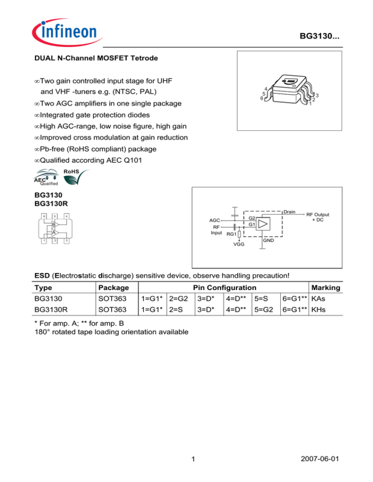
BG3130
BG3130R
Drain
$
#
"
AGC
RF
Input RG1
*
)
G2
G1
RF Output
+ DC
GND
!
VGG
ESD (Electrostatic discharge) sensitive device, observe handling precaution!
Type
Package
Pin Configuration
Marking
BG3130
SOT363
1=G1* 2=G2
3=D*
4=D**
5=S
6=G1** KAs
BG3130R
SOT363
1=G1* 2=S
3=D*
4=D**
5=G2
6=G1** KHs
* For amp. A; ** for amp. B
180° rotated tape loading orientation available
1
2007-06-01
BG3130...
Maximum Ratings
Parameter
Symbol
Drain-source voltage
VDS
Continuous drain current
ID
Gate 1/ gate 2-source current
±IG1/2SM
1
Gate 1/ gate 2-source voltage
±V G1/G2S
6
Total power dissipation
Ptot
200
Storage temperature
Tstg
-55 ... 150
Channel temperature
Tch
150
Value
8
25
Unit
V
mA
V
mW
°C
Thermal Resistance
Parameter
Symbol
Value
Unit
Channel - soldering point1)
Rthchs
≤ 280
K/W
1For
calculation of RthJA please refer to Application Note Thermal Resistance
2
2007-06-01
BG3130...
Electrical Characteristics at TA = 25°C, unless otherwise specified
Parameter
Symbol
Values
Unit
min.
typ.
max.
V(BR)DS
12
-
-
+V(BR)G1SS
6
-
15
+V(BR)G2SS
6
-
15
+IG1SS
-
-
50
µA
+IG2SS
-
-
50
nA
IDSS
-
-
10
µA
IDSX
-
10
-
mA
VG1S(p)
-
0.7
-
V
VG2S(p)
-
0.6
-
DC Characteristics
Drain-source breakdown voltage
V
ID = 10 µA, VG1S = 0 V, VG2S = 0 V
Gate1-source breakdown voltage
+IG1S = 10 mA, V G2S = 0 V, VDS = 0 V
Gate2-source breakdown voltage
+IG2S = 10 mA, V G1S = 0 V, VDS = 0 V
Gate1-source leakage current
VG1S = 6 V, VG2S = 0 V
Gate2-source leakage current
VG2S = 8 V, VG1S = 0 V, VDS = 0 V
Drain current
VDS = 5 V, VG1S = 0 V, VG2S = 4.5 V
Drain-source current
VDS = 5 V, VG2S = 4 V, RG1 = 120 kΩ
Gate1-source pinch-off voltage
VDS = 5 V, VG2S = 4 V, ID = 20 µA
Gate2-source pinch-off voltage
VDS = 5 V, I D = 20 µA
3
2007-06-01
BG3130...
Electrical Characteristics at TA = 25°C, unless otherwise specified
Parameter
Symbol
Values
min.
typ.
Unit
max.
AC Characteristics V DS = 5V, V G2S = 4V, (ID = 14 mA) (verified by random sampling)
Forward transconductance
gfs
-
33
-
mS
Gate1 input capacitance
Cg1ss
-
1.9
-
pF
Cdss
-
1.1
-
f = 10 MHz
Output capacitance
f = 10 MHz
Power gain
Gp
dB
f = 800 MHz
-
24
-
f = 45 MHz
-
31
-
Noise figure
dB
F
f = 800 MHz
-
1.3
-
f = 45 MHz
-
1.7
-
45
-
-
∆G p
Gain control range
VG2S = 4 ... 0 V, f = 800 MHz
Cross-modulation k=1%, fw=50MHz, funw=60MHz Xmod
-
AGC = 0 dB
90
-
-
AGC = 10 dB
-
87
-
AGC = 40 dB
96
100
-
4
2007-06-01
BG3130...
Total power dissipation Ptot = ƒ(TS)
amp. A = amp. B
Drain current ID = ƒ(IG1)
VG2S = 4V
amp. A = amp. B
300
30
mA
200
20
ID
P tot
mW
150
15
100
10
50
5
0
0
20
40
60
80
100
120 °C
0
0
150
10
20
30
40
50
60
70
80 µA
100
IG1
TS
Output characteristics ID = ƒ(V DS)
amp. A = amp. B
Gate 1 current IG1 = ƒ(V G1S)
VDS = 5V, VG2S = Parameter
amp. A = amp. B
225
22
mA
1.3V
µA
4V
18
175
1.2V
14
VG1S
ID
16
1.1V
3.5V
150
125
12
3V
1V
10
100
8
75
2.5V
6
50
0.8V
4
2V
25
2
0
0
2
4
6
8
10
V
0
0
14
VDS
0.4
0.8
1.2
1.6
2
2.4
V
3.2
IG1
5
2007-06-01
BG3130...
Drain current ID = ƒ(V G1S)
VDS = 5V, VG2S = Parameter
Gate 1 forward transconductance
g fs = ƒ(ID), VDS = 5V, VG2S = Parameter
amp. A = amp. B
amp. A = amp. B
40
32
mS
4V
µA
3V
4V
30
24
2.5V
ID
g fs
3.5V
25
20
3V
20
16
2V
15
12
2.5V
2V
10
8
1.5V
5
0
0
4
4
8
12
16
20
24
28 mA
0
0
36
0.2 0.4 0.6 0.8
1
1.2 1.4 1.6
ID
V
2
VG1S
Drain current ID = ƒ(VGG ) amp.A=amp.B
Drain current ID = ƒ(VGG)
VDS = 5V, VG2S = 4V, RG1 = 120kΩ
VG2S = 4V, RG1 = Parameter in kΩ
(connected to VGG, VGG =gate1 supply voltage)
amp. A = amp. B
13
mA
22
70
mA
80
11
18
10
ID
ID
100
16
9
8
7
12
6
10
5
120
14
8
4
6
3
4
2
2
1
0
0
0.5
1
1.5
2
2.5
3
3.5
4
V
0
0
5
VGG
1
2
3
4
5
V
7
VGG=VDS
6
2007-06-01
BG3130...
Crossmodulation Vunw = (AGC)
VDS = 5 V, Rg1 = 68 kΩ
120
V unw
dBµV
100
90
80
0
10
20
30
dB
50
AGC
7
2007-06-01
BG3130...
Crossmodulation test circuit
VAGC
VDS
4n7
R1
10kΩ
2.2 uH
4n7
4n7
RL
50Ω
RGEN
50Ω
4n7
50 Ω
RG1
VGG
Semibiased
8
2007-06-01
Package SOT363
BG3130...
Package Outline
2 ±0.2
0.9 ±0.1
+0.1
6x
0.2 -0.05
0.1
0.1 MAX.
M
0.1
Pin 1
marking
1
2
3
A
1.25 ±0.1
4
0.1 MIN.
5
2.1 ±0.1
6
0.15 +0.1
-0.05
0.65 0.65
0.2
M
A
Foot Print
1.6
0.9 0.7
0.3
0.65
0.65
Marking Layout (Example)
Small variations in positioning of
Date code, Type code and Manufacture are possible.
Manufacturer
2005, June
Date code (Year/Month)
Pin 1 marking
Laser marking
BCR108S
Type code
Standard Packing
Reel ø180 mm = 3.000 Pieces/Reel
Reel ø330 mm = 10.000 Pieces/Reel
For symmetric types no defined Pin 1 orientation in reel.
0.2
2.3
8
4
Pin 1
marking
1.1
2.15
9
2007-06-01
BG3130...
Edition 2006-02-01
Published by
Infineon Technologies AG
81726 München, Germany
© Infineon Technologies AG 2007.
All Rights Reserved.
Attention please!
The information given in this dokument shall in no event be regarded as a guarantee
of conditions or characteristics (“Beschaffenheitsgarantie”). With respect to any
examples or hints given herein, any typical values stated herein and/or any information
regarding the application of the device, Infineon Technologies hereby disclaims any
and all warranties and liabilities of any kind, including without limitation warranties of
non-infringement of intellectual property rights of any third party.
Information
For further information on technology, delivery terms and conditions and prices
please contact your nearest Infineon Technologies Office (www.infineon.com).
Warnings
Due to technical requirements components may contain dangerous substances.
For information on the types in question please contact your nearest
Infineon Technologies Office.
Infineon Technologies Components may only be used in life-support devices or
systems with the express written approval of Infineon Technologies, if a failure of
such components can reasonably be expected to cause the failure of that
life-support device or system, or to affect the safety or effectiveness of that
device or system.
Life support devices or systems are intended to be implanted in the human body,
or to support and/or maintain and sustain and/or protect human life. If they fail,
it is reasonable to assume that the health of the user or other persons
may be endangered.
10
2007-06-01


