Technology Solutions
Copper (Cu) Wire Bonding
Copper (Cu) wire has
long been used as a
method of connecting a
silicon die to the
package terminals.
With the recent
increase in gold (Au)
wire cost, Cu wire is an
attractive way to
manage overall
package cost.
Copper Wire Benefits
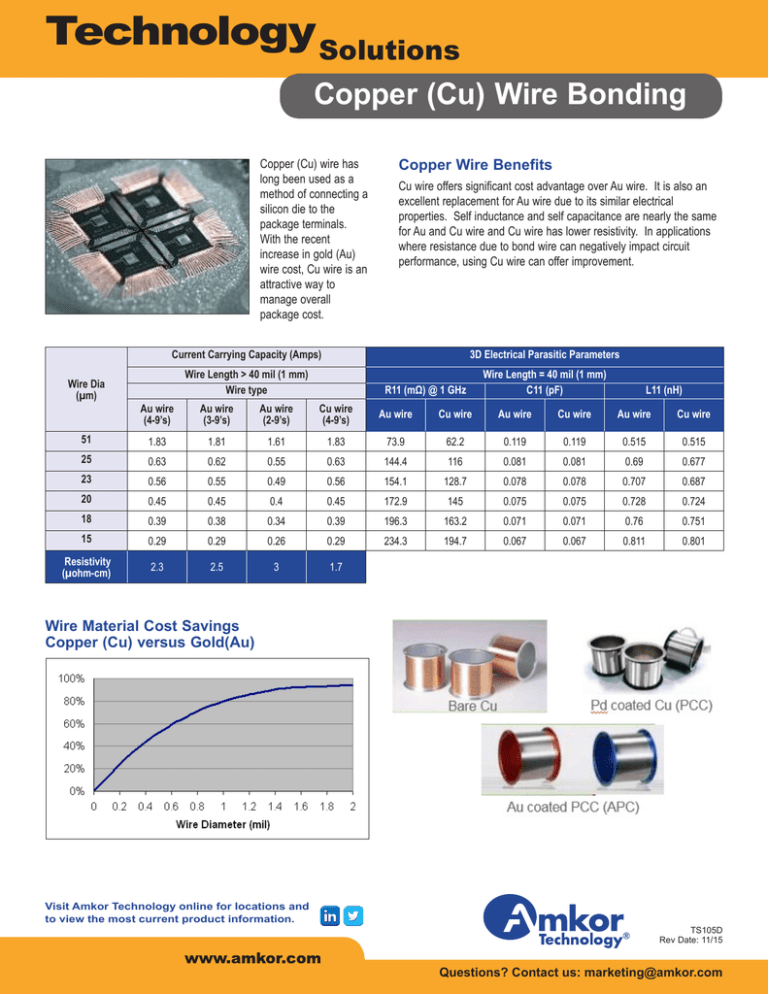
Cu wire offers significant cost advantage over Au wire. It is also an
excellent replacement for Au wire due to its similar electrical
properties. Self inductance and self capacitance are nearly the same
for Au and Cu wire and Cu wire has lower resistivity. In applications
where resistance due to bond wire can negatively impact circuit
performance, using Cu wire can offer improvement.
Current Carrying Capacity (Amps)
Wire Dia
(µm)
3D Electrical Parasitic Parameters
Wire Length > 40 mil (1 mm)
Wire type
R11 (mΩ) @ 1 GHz
Wire Length = 40 mil (1 mm)
C11 (pF)
L11 (nH)
Au wire
(4-9’s)
Au wire
(3-9’s)
Au wire
(2-9’s)
Cu wire
(4-9’s)
Au wire
Cu wire
Au wire
Cu wire
Au wire
Cu wire
51
1.83
1.81
1.61
1.83
73.9
62.2
0.119
0.119
0.515
0.515
25
0.63
0.62
0.55
0.63
144.4
116
0.081
0.081
0.69
0.677
23
0.56
0.55
0.49
0.56
154.1
128.7
0.078
0.078
0.707
0.687
20
0.45
0.45
0.4
0.45
172.9
145
0.075
0.075
0.728
0.724
18
0.39
0.38
0.34
0.39
196.3
163.2
0.071
0.071
0.76
0.751
15
0.29
0.29
0.26
0.29
234.3
194.7
0.067
0.067
0.811
0.801
Resistivity
(µohm-cm)
2.3
2.5
3
1.7
Wire Material Cost Savings
Copper (Cu) versus Gold(Au)
Visit Amkor Technology online for locations and
to view the most current product information.
TS105D
Rev Date: 11/15
Questions? Contact us: marketing@amkor.com
Technology
Copper (Cu) Wire Bonding
Solutions
Minimum Bond Pad Size by Wire Diameter (T = Bond Pad Metal Thickness)
Wire
(µm)
Recommended
Minimum
0.7 ≤ T ≤ 1.5 µm
FWD
1.6 ≤ T ≤ 2.5 µm
SSB
FWD
2.6 ≤ T ≤ 4.0 µm
SSB
FWD
SSB
BPO
BPP
BPO
BPP
BPO
BPP
BPO
BPP
BPO
BPP
BPO
BPP
15
≥35
≥40
≥39
≥46
≥37
≥42
≥42
≥49
≥39
≥44
≥44
≥51
18
≥40
≥45
≥45
≥52
≥42
≥47
≥48
≥55
≥44
≥49
≥50
≥57
20
≥44
≥50
≥49
≥57
≥46
≥52
≥52
≥60
≥48
≥54
≥54
≥62
23
≥52
≥58
≥57
≥65
≥54
≥60
≥60
≥68
≥56
≥62
≥62
≥70
25
≥56
≥62
≥62
≥70
≥58
≥64
≥65
≥73
≥60
≥66
≥67
≥75
15
≥34
≥38
≥38
≥45
≥36
≥40
≥40
≥47
≥37
≥41
≥42
≥49
18
≥39
≥43
≥44
≥51
≥41
≥45
≥46
≥53
≥42
≥46
≥48
≥55
20
≥43
≥47
≥48
≥56
≥45
≥49
≥50
≥58
≥46
≥50
≥52
≥60
23
≥51
≥55
≥56
≥64
≥52
≥56
≥58
≥66
≥54
≥58
≥60
≥68
25
≥55
≥59
≥61
≥69
≥56
≥60
≥63
≥71
≥58
≥62
≥65
≥73
Wafer Technology Node and Cu Wire Readiness
>60 nm
55/60 nm
45/40 nm
28 nm
<28 nm
Non-Low-K or Low-K
Low-K
Low-K
Ultra Low-K
Ultra Low-K
Ultra Low-K
Reliability Status
Customer Qualified
Customer Qualified
Customer Qualified
Customer Qualified
In Process
Production Status
HVM
HVM
HVM
HVM
Development
Package Family and Factory Qualification
Package Family
Cu Wire HVM Plant
CABGA
C3, K4, P3, J1
LQFP
K1, P1, T1, J1
MLF
C3, K1, P3
MQFP
P1, T1
PBGA
C3, K4, P3
PDIP
P1
PLCC
P1
PSOP
P1
SC70
P1
SCSP
C3, K4, J1
SOIC
P1
SOT-23
P1
SSOP
P1
TQFP
K1, P1, T1, J1
TSSOP
P1
Visit Amkor Technology online for locations and
to view the most current product information.
With respect to the information in this document, Amkor makes no guarantee or warranty of its accuracy or that the use of such information will not infringe upon the intellectual rights of third parties. Amkor shall not
be responsible for any loss or damage of whatever nature resulting from the use of, or reliance upon it and no patent or other license is implied hereby. This document does not in any way extend or modify Amkor’s
warranty on any product beyond that set forth in its standard terms and conditions of sale. Amkor reserves the right to make changes in its product and specifications at any time and without notice. The Amkor name
and logo are registered trademarks of Amkor Technology, Inc. All other trademarks mentioned are property of their respective companies. © 2015, Amkor Technology Incorporated. All Rights Reserved.
TS105D
Rev Date: 11/15
Questions? Contact us: marketing@amkor.com
