3 High Performance Multilayer Printed Circuit Boards
advertisement

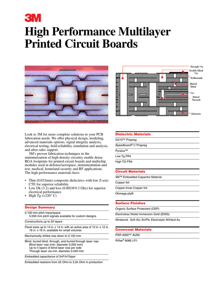
3 High Performance Multilayer Printed Circuit Boards Look to 3M for more complete solutions to your PCB fabrication needs. We offer physical design, modeling, advanced materials options, signal integrity analysis, electrical testing, field reliability simulation and analysis, and after-sales support. 3M’s proven fabrication techniques in the miniaturization of high density circuitry enable dense BGA footprints for printed circuit boards and multichip modules used in defense/aerospace, instrumentation and test, medical, homeland security and RF applications. The high performance materials have: • Thin (0.032mm) composite dielectrics with low Z-axis CTE for superior reliability • Low Dk (3.2) and loss (0.002@9.3 Ghz) for superior electrical performance • High Tg (>220° C) Design Summary 0.100 mm pitch trace/space 0.050 mm pitch signals available for custom designs Constructions up to 25 layers Dielectric Materials G410™ Prepreg Speedboard® C Prepreg Pyralux™ Low Tg FR4 High TG FR4 Circuit Materials 3M™ Embedded Capacitor Material Copper foil Copper-Invar-Copper foil Ohmega-ply® Surface Finishes Organic Surface Protectant (OSP) Electroless Nickel Immersion Gold (ENIG) Wirebond: Soft AU; Sn/Pb; Electrolytic Ni/Hard Au Panel sizes up to 14 in. x 14 in. with an active area of 12 in. x 12 in. 16 in. x 16 in. available for small volumes Covercoat Materials Mechanically drilled vias down to 0.150 mm PSR 4000™ AUS5 Blind, buried blind, through, and buried through laser vias Blind laser vias (min. diameter 0.050 mm) Up to 4 layers of blind laser vias per side Through laser via min. diameter 0.040 mm R/flex® 8080 LP1 Embedded capacitance of 5nF/in2/layer Embedded resistors from 25 Ohm to 3.2k Ohm in production Product Feature Properties Standard Metric (mm) Advanced Custom Standard English (mils) Advanced Custom Cu Thickness Min. 0.005 0.005 0.003 1/7 oz. 1/7 oz. 1/12 oz. Cu Thickness Max. 0.035 0.035 0.140 1 oz. 1 oz. 4 oz. Internal Lines Min - 1/3oz Cu 0.062 0.050 0.020 2.4 2.0 0.8 Internal Spaces Min - 1/3oz Cu 0.062 0.050 0.030 2.4 2.0 1.2 External Lines Min - 1/3oz Cu 0.062 0.050 0.020 2.4 2.0 0.8 External Spaces Min - 1/3oz Cu 0.062 0.050 0.040 2.4 2.0 1.6 Minimum Pitch for Full BGA 0.800 0.500 0.400 31.5 19.7 15.7 Minimum SMT Pitch 0.300 0.225 0.100 11.8 8.9 3.9 Pad Over Drill Size (Laser) 0.050 0.040 0.030 2.0 1.6 1.2 Pad Over Drill Size (Drill) 0.200 0.125 0.125 7.9 4.9 4.9 Soldermask Registration (+/-) 0.065 0.050 0.020 2.6 2.0 0.8 Soldermask Min. Web 0.100 0.075 0.050 3.9 3.0 2.0 Soldermask Min. Clearance 0.100 0.075 0.025 3.9 3.0 1.0 Soldermask Feature Size (+/-) 0.020 0.010 0.005 0.8 0.4 0.2 Flip Chip on Board Pitch Min. 0.200 Flip Chip on Board Pad Size Min. 0.090 Routed Feature Edge (+/-) Drilled Via Properties 0.127 0.100 0.010 Metric (mm) Standard Advanced Custom 7.9 3.5 5.0 3.9 0.4 English (mils) Standard Advanced Custom Via Aspect Ratio 10:1 15:1 20:1 10:1 15:1 20:1 Buried Through Via Diameter Min. 0.200 0.150 0.150 7.9 5.9 5.9 Through Via Diameter Min. 0.200 0.150 0.150 7.9 5.9 5.9 Laser Microvia Properties Standard Metric (mm) Advanced Custom Standard English (mils) Advanced Custom Multidepth Microvias Yes Yes Yes Yes Yes Buried Microvias Yes Yes Yes Yes Yes Yes Blind Microvia Aspect Ratio 1.3:1 1.3:1 1.3:1 1.3:1 1.3:1 1.3:1 Blind Minimum 0.050 0.050 0.050 2.0 2.0 2.0 Buried Blind Minimum 0.050 0.050 0.050 2.0 2.0 2.0 4 4 4+ 4 4 4+ 10:1 15:1 20:1 10:1 15:1 20:1 Max. Layers of Blind Vias/Side Through Via Aspect Ratio Max.Contact Layers at Max AR Yes 8 4 2 8 4 2 Through Via Min. Diameter 0.060 0.050 0.040 2.4 2.0 1.6 Buried Through Min. Diameter 0.060 0.050 0.040 2.4 2.0 1.6 17 17 25 17 17 25 Through Via Max. Layers Pyralux is a registered trademark of DuPont. G410 and Speedboard are registered trademarks of W.L. Gore & Associates. Ohmega-ply is a registered trademark of Ohmega Technologies, Inc. PSR 4000 is a registered trademark of Taiyo. R/flex is a registered trademark of Rogers Corporation. 3M is a registered trademark of 3M Company. Important Notice Before using this product, you must evaluate it and determine if it is suitable for your intended application. You assume all risks and liability associated with such use. Warranty; Limited Remedy; Limited Liability. 3M’s product warranty is stated in its Product Literature available upon request. 3M MAKES NO OTHER WARRANTIES INCLUDING, BUT NOT LIMITED TO, ANY IMPLIED WARRANTY OF MERCHANTABILITY OR FITNESS FOR A PARTICULAR PURPOSE. If this product is defective within the warranty period stated above, your exclusive remedy shall be, at 3M’s option, to replace or repair the 3M product or refund the purchase price of the 3M product. Except where prohibited by law, 3M will not be liable for any indirect, special, incidental or consequential loss or damage arising from this 3M product, regardless of the legal theory asserted. 3 3M Electronics 6801 River Place Blvd. Austin, TX 78726-9000 800 676 8381 www.3M.com/electronics Recycled Paper 40% Pre-consumer waste paper 10% Post-consumer waste paper Litho in USA. © 3M 2005 80-6201-3604-0


