VOL. 11, NO. 5, MARCH 2016
ARPN Journal of Engineering and Applied Sciences
ISSN 1819-6608
©2006-2016 Asian Research Publishing Network (ARPN). All rights reserved.
www.arpnjournals.com
RF SWITCHES IN WIDE-, BROAD-, AND MULTI-BAND RF FRONT-END
OF WIRELESS COMMUNICATIONS: AN OVERVIEW
A. M. S. Zobilah, N. A. Shairi, Z. Zakaria and M. S. Jawad
Centre for Telecommunication Research & Innovation (CeTRI), Faculty of Electronics and Computer Engineering, Universiti Teknikal
Malaysia Melaka (UTeM), Hang Tuah Jaya, Durian Tunggal, Melaka, Malaysia
E-Mail: zobilah12@hotmail.com
ABSTRACT
This paper presents an important overview on the RF switches for wide-band, broad-band and multi-band RF
front-end of wireless communications. This paper is mainly focused on the discussion of the circuit configuration of RF
switches that using Time Division Duplex (TDD) switching in wireless communications such as WiMAX, WiFi and LTE.
The previous research works on the RF switches for wide-band, broad-band and multi-band RF front-end are discussed in
term of technology used, circuit design, performance and its applications.
Keywords: RF switch, SPDT switch, wide-band, broad-band, multi-band.
INTRODUCTION
In modern wireless communication, there is a
requirement of designing a wide-, broad- or multi-band RF
front-end. It requires wide-, broad- or multi-band RF
subcomponents in the RF front-end to support different
band and different standard (e.g. WiFi, WiMAX, LTE,
WiBro, HiperLAN and etc.). Therefore, these have created
new challenges to circuit and system designers in
developing a wide-, broad- or multi-band RF front-end
system. Several wide-, broad- or multi-band RF
subcomponents can be found in antenna [1], [2], filter [3],
[4] and amplifier designs [5], [6].
Take an example in WiMAX system. This system
uses Time Division Duplex (TDD) communication at
different frequency band such as 2.3, 3.5 and 5.5 GHz
bands. These bands are set within 2-6 GHz range for
mobile WiMAX and 2-11 GHz range for fixed WiMAX
[7]. Hence, it is valuable if the RF front-end is less
expensive and/or smaller than simply putting multiple RF
components next to each other that has acceptable
performance. Moreover, the integration of multiple
wireless systems might be required either for different
standards (e.g. WiFi and WiMAX) or different spectrum
allocations at various locations (e.g. different WiMAX
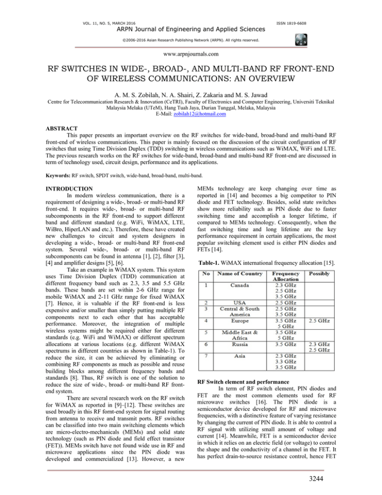
spectrums in different countries as shown in Table-1). To
reduce the size, it can be achieved by eliminating or
combining RF components as much as possible and reuse
building blocks among different frequency bands and
standards [8]. Thus, RF switch is one of the solution to
reduce the size of wide-, broad- or multi-band RF frontend system.
There are several research work on the RF switch
for WiMAX as reported in [9]–[12]. These switches are
used broadly in this RF fornt-end system for signal routing
from antenna to receive and transmit ports. RF switches
can be classified into two main switching elements which
are micro-electro-mechanicals (MEMs) and solid state
technology (such as PIN diode and field effect transistor
(FET)). MEMs switch have not found wide use in RF and
microwave applications since the PIN diode was
developed and commercialized [13]. However, a new
MEMs technology are keep changing over time as
reported in [14] and becomes a big competitor to PIN
diode and FET technology. Besides, solid state switches
show more reliability such as PIN diode due to faster
switching time and accomplish a longer lifetime, if
compared to MEMs technology. Consequently, when the
fast switching time and long lifetime are the key
performance requirement in certain applications, the most
popular switching element used is either PIN diodes and
FETs [14].
Table-1. WiMAX international frequency allocation [15].
RF Switch element and performance
In term of RF switch element, PIN diodes and
FET are the most common elements used for RF
microwave switches [16]. The PIN diode is a
semiconductor device developed for RF and microwave
frequencies, with a distinctive feature of varying resistance
by changing the current of PIN diode. It is able to control a
RF signal with utilizing small amount of voltage and
current [14]. Meanwhile, FET is a semiconductor device
in which it relies on an electric field (or voltage) to control
the shape and the conductivity of a channel in the FET. It
has perfect drain-to-source resistance control, hence FET
3244
VOL. 11, NO. 5, MARCH 2016
ARPN Journal of Engineering and Applied Sciences
ISSN 1819-6608
©2006-2016 Asian Research Publishing Network (ARPN). All rights reserved.
www.arpnjournals.com
switches are more stable an repeatable to PIN diode [14].
Besides, emerging MEMs switch technology attempts to
apply the advantages of conventional electro-mechanicals
(EMs) switches, but in a small size. MEMS switches
employ micro-miniaturized mechanical contacts controlled
by electrostatic forces to make RF connections [17].
Generally, the switch performance can be shown
by describing its key parameters such as insertion loss,
isolation and switching speed [16]. Insertion loss is a
power loss ratio of a signal between output and input of
RF switch element during the ON state. For instance, as
reported in [14] insertion loss is a discriminating detail of
a switch in system applications that expect an extra power
to recompense for the loss that is not available.
Meanwhile, isolation is defined as the ratio of the power
level when the switch’s path is OFF to the power level
when the switch is ON. Perfect isolation keeps stray
signals from leaking into the desired state, whether ON or
OFF. Switching speed is a time expected to convert the
condition of a switch from ON state to OFF state or vice
versa. It is usually described in two ways: on/off time and
rise/fall time.
In applications such as mobile handsets, which
need to handle a large number of different signals, and
different frequency bands, it needs RF switches with
multiple throw such as single pole four throw (SP4T),
single pole seven throw (SP7T) or single pole nine throw
(SP9T) as reported in [20], [21]. Furthermore, it can
simpliying the mobile handsets [22]. In this application, it
introduced different implementation of RF front-end:
discrete, hybrid and mixed RF front-end designs. As the
target application for these designs was smart phones, so
the discrete solution of RF front-end was not well-suited.
RF SWITCH FOR WIDE-, BROAD- AND MULTIBAND RF FRONT-END
Figure-2. Configuration B: narrow-band RF switches in
RF front-end system.
RF Switch configurations
In RF switch configurations in TDD
communication, there are three techniques to design the
switch for wide-, broad and multi-band applications. An
example is taken from WiMAX with three frequency
bands, 2.3, 3.5 and 5.5 GHz. As shown in Figure-1, the
configuration A uses a single wide, broad- or multi-band
single pole double throw (SPDT) switch that connected to
transmitter (Tx) and receiver (Rx) chains. Both double
throw ports have a triplexer to separate three different
frequency bands. Meanwhile, the configuration B in
Figure-2 consists of triplexer and three narrow-band SPDT
switches operating at three different frequencies (2.3, 3.5
and 5.5 GHz). In this configuration, a single triplexer is
used to separate the three different frequency bands. The
configuration C in Figure-3 consists of single RF switch
which is single pole six throw (SP6T) to switch at
different frequency bands at different time. In this
configuration, the six throw uses single frequency band
[18], [19].
Figure-1. Configuration A: wide-, broad- and multi-band
RF switches in RF front-end system.
Figure-3. Configuration C: multi-throw narrow-band RF
switch in RF front-end system.
Related research works
From literatures, several key designs of RF
switches for wide-, broad- and multi-band application are
discussed in this section. Most of the research works were
focused on the wide- and broad-band RF switches such as
in [23]–[26] but there is a few research works on multiband RF switch such as reported in [27]. Designing wide-,
and broad-band RF switches are more challenging
compared to narrow-band RF switches. It requires very
wide- or broad-band of isolation, insertion loss and return
loss. Meanwhile for the multi-band RF switches, it
requires to consider the harmonics of each band from
distorting the other bands.
Table-2 is the lists of the related and selected
research works on the RF switches for wide-, broad- and
multi-band application.
An ultrafast wideband low-loss SPDT switch
using SiGe bipolar technique was reported in [23]. The
authors used HBT transistors as a switch elements in order
3245
VOL. 11, NO. 5, MARCH 2016
ARPN Journal of Engineering and Applied Sciences
ISSN 1819-6608
©2006-2016 Asian Research Publishing Network (ARPN). All rights reserved.
www.arpnjournals.com
to introduce a configuration of adopting current steering
technology. It produced a measured switching time of 75
per second, which recommends a most extreme switching
rate of 13 Gb/s in V-band. In this paper, common-emitter
topology was offered with the target to minimize the noise
figure. As a result, this paper shows less than 1.25 dB
insertion loss, about 10 dB return loss and greater than 18
dB isolation from 42 GHz to 70 GHz.
Authors in [24] presented an ultra low-loss 50-70
GHz SPDT switch using 90 nm CMOS technique with
FET transistors as switch elements. The circuit consists of
λ/4 transmission lines with shunt inductors at the output
matching network. To accomplish low insertion loss, this
paper used high substrate resistance contacts. As results, it
produced less than 2 dB insertion loss, higher than 25 dB
isolation and higher than -8 dB return loss from 50 to70
GHz. The layout area is 0.5x0.55 mm2 which, by folding
the λ/4 transmission lines. This design shows the lowest
insertion loss, if compared with other switches using the
same technology.
Table-2. Related and selected research works on the RF
switches for wide-, broad- and multi-band application.
Authors in [28] reported two switches, one is
SPST and the other is SPDT. Both switches were proposed
that operated from 57 to 66 GHz. In this paper, the circuit
was fabricated using 65nm CMOS technology. The SPDT
design achieved higher than 21 dB, higher than 10 dB and
about 3 dB, for isolation, return loss and insertion loss
respectively. Meanwhile, the SPST design produced a
good result for isolation and return loss. On the other
hand, several CMOS transceiver/receiver switches have
been discussed in [29], [30]. However, the performance of
RF switch in [30] is not that good for the typical design of
shunt-series configuration [28].
In addition, authors in [25] proposed a design of
SPDT switch for broadband using PIN diodes. WiMAX,
LTE and etc. are the examples of where the proposed
design can be applied from 0.5 to 3 GHz. The RF switch
was built using PIN diodes of HSMP-389Y. Besides, it is
a challenge to achieve good isolation result by using only
a single packaged of PIN diode [31], unless circuit design
techniques are implimented. As results, isolation higher
than 25 dB and insertion loss of 1 dB were achieved.
Moreover, in [32] two different configuration
SPDT switches at frequency from 8.5 to 10.5 GHz were
reported. The designs were fabricated using 0.13 um SiGe
BiCMOS technology with nMOS transistors as switch
elements. In this paper, the two designs can be described
as follows. One is shunt configuration using λ/4 sections
and the other is series-shunt configuration using matching
networks. As results, the first design produced 20.5 dB
isolation, 1.89 dB insertion loss and 14.5 dB return loss.
The second design produced returns loss, insertion loss,
and isolation of 22.2 dB, 2.33 dB, and 22.5 dB
respectively. It is found that the switches worked as the
same as other CMOS switches which are using nonstandard processes.
Meanwhile, in [26], SPDT switch using CMOS
technology was designed. Authors used switch elements of
MOS transistors and body-floating technique in order to
increase the linearity and decrease the insertion loss. In
addition, to increase isolation, the leakage cancellation
technique was used. In measurement results, the switch
showed that the isolation is higher than 28 dB and the
insertion loss is less than 3.5 dB from 57 to 64 GHz. The
proposed design has a good result in terms of return loss,
insertion loss and isolation (34 dB) at the center
frequency. Also it is observed that the RF switch has a
good flatness response of the input 1-dB compression
point (IP1dB) of 6.5 to 6.9 dBm at the operation frequency
from 57 to 64 GHz. Moreover, the design is useful for the
RF front-end integration in 60-GHz CMOS single-chip RF
transceiver.
A low loss high isolation broadband single-port
double-throw (SPDT) traveling-wave switch using 90 nm
CMOS technology was proposed in [33]. In this paper,
nMOS transistors was used with body bias technique to
improve the circuit performance of the switch, especially
for the operation frequency greater than 30 GHz.
Moreover, the input P1dB and IMD of the SPDT switch
are both enhanced by 2 and 10 dB at 20 GHz, respectively.
3246
VOL. 11, NO. 5, MARCH 2016
ARPN Journal of Engineering and Applied Sciences
ISSN 1819-6608
©2006-2016 Asian Research Publishing Network (ARPN). All rights reserved.
www.arpnjournals.com
Also, the loss and the linearity of the circuit are improved
due to the reduction of the capacitance in the cold-mode
state. As result, the switch showed an insertion loss of 3
dB and an isolation of higher than 48 dB from DC to 60
GHz. To the best of the authors’ knowledge, this work is
the widest 3 dB bandwidth among others that uses CMOS
SPDT technology.
Adding to that, design in [34] is a bandpass
SPDT filter-integrated switches using FET transistors.
Authors provided a technique integrating an SPDT switch
with a quarter-wavelength bandpass filter. In this paper,
two SPDT switches were fabricated to validate the design
concept; one is hybrid circuit (at 1 GHz) and the other is
monolithic-microwave integrated-circuit (MMIC) (at 60
GHz). Both switches achieved 30% FBW and suitable for
wide-band communication system. As a result, the hybrid
switch exhibited 20 dB isolation and 1.5 dB insertion loss,
at center frequency. Furthermore, the MMIC switch
showed that the insertion loss was lower than 2.5 dB and
the isolation was higher than 27 dB. In addition, the
method used in this paper provides a simple and precise
way to obtain the power compression point and the
dominant components without generating nonlinear
models and nonlinear simulation tools, which is useful to
design for the power performance of SPDT switches.
Meanwhile, authors in [27] designed an SPDT
switch for multi frequency bands with ladder circuits. This
design used PIN diodes to operate with multi-band
frequencies in order to be applicable for three wireless
applications in 1.6 GHz, 2.5 GH and 5.8 GHz band for
global positioning system (GPS), vehicle information and
communication system (VICS), and a dedicated shortrange communication system/electric toll collection
system (DSRC/ETC). On the other hand, this paper
introduced a ladder circuit with simple configuration and
low cost. Authors fabricated two types of switches;
lumped circuit elements and semi-microstrip elements. As
result, the variations on the second switch are about 25%
of those of the first design. The circuit produced isolation
higher than 20 dB and less than 2 dB of insertion loss. The
proposed design is a key gadget to bi-directional multiband automobile communication systems.
CONCLUSIONS
From literatures, there is a demand on the RF
switches for wide-, broad- and multi-band RF front-end
for wireless communication systems. The purpose is to
support different band and different standard (e.g. WiFi,
WiMAX, LTE, WiBro, HiperLAN and etc.). Three
options of configuration of RF switches for wide-, broadand multi-band RF front-end were discussed that consist
of filter and triplexer. In general, these RF switches for
wide-, broad- and multi-band RF front-end are essential to
eliminate sub-component and thus reduce the size of RF
front-end system.
ACKHNOWLEDGEMENTS
We would like to acknowledge the contribution
of our colleagues from Faculty of Electronics and
Computer Engineering, Universiti Teknikal Malaysia
Melaka (UTeM) for preparing of this review paper.
REFERENCES
[1] F. Malek, N. A. Zainuddin, M. Z. A. Abd Aziz, H.
Nornikman, B. H. Ahmad, M. F. A. Malek, and M. A.
Othman. 2013. Double C-shaped monopole antenna
array for dual band WLAN application. IEEE Symp.
Wirel. Technol. Appl. ISWTA. pp. 274–279.
[2] Abd Aziz, M.Z.A.; Shukor, M.M.; Suaidi, M.K.;
Ahmad, B.H.; Othman, M.A.; Hasan, N. 2013. Design
a 3.5 slot antenna using coplanar waveguide (CPW)
for dual band application. Microwave Techniques
(COMITE), 2013l Conference on. pp. 31-35.
[3] Z. Zakaria, M. A. Mutalib, M. S. Mohamad Isa, and
N. A. Zainuddin. 2013. Transformation of generalized
chebyshev lowpass filter prototype to Suspended
Stripline Structure highpass filter for wideband
communication systems. 2013 IEEE Int. Conf. RFIDTechnologies Appl. RFID-TA. pp. 1–5.
[4] Z. Zakaria, M. A. Mutalib, W. Y. Sam, A. R. Othman,
M. F. M. Fadzil, A. A. M. Bakar, and N. Saifullah.
2015. A Compact Structure of S-Shape Bandpass
Filter for Wideband Applications. Adv. Sci. Lett..
21(1): 39–41.
[5] P. Ho, Y. Lin, H. Wang, and C. Meliani. 2014. A
Broadband 75 to 140 GHz Amplifier in 0 . 13- μ m
SiGe HBT Process. Proceedings of the 44th European
Microwave Conference. pp. 1368–1371.
[6] A. R. Othman, A. H. Hamidon, M. N. Husain, M. S.
Johal, and A. B. Ibrahim. 2011. Wideband 5.8 GHz
Radio Frequency Amplifier with 3 dB ∏-Network
Attenuator Isolation. J. Telecommun. Electron.
Comput. Eng. 3(1): 1–6.
[7] CCM.net. 2015. WiMAX - 802.16 - Worldwide
Interoperability for Microwave Access.
[8] C. Bowick. 2008. What’s in an RF Front End? EE
Times.
[9] R. Phudpong, N. Youngthanisara, P. Kukieattikool,
M. Kitjaroen, and S. Siwamogsatham. 2012. An
absorptive bandpass-integrated p-i-n diode T/R switch
for 2.5 GHz WiMAX high power terminals. Microw.
Opt. Technol. Lett. 54(12): 2705–2708.
[10] N. A. Shairi, B. H. Ahmad, and P. W. Wong. 2013.
SPDT Discrete Switch Design using Switchable
Radial Stub Resonator for WiMAX and LTE in 3.5
GHz Band. RF and Microwave Conference (RFM),
2013 IEEE International. pp. 1–5.
3247
VOL. 11, NO. 5, MARCH 2016
ARPN Journal of Engineering and Applied Sciences
ISSN 1819-6608
©2006-2016 Asian Research Publishing Network (ARPN). All rights reserved.
www.arpnjournals.com
[11] D. J. S. M. and C. C. Lim. 2010. Design A SPDT
Switch For WiMAX. Microwaves and RF.
[12] N. A. Shairi, P. W. Wong, and B. H. Ahmad. 2014.
Switchable matched ring resonator in SPDT discrete
switch design for WiMAX and LTE in 3.5 GHz band.
in Asia-Pacific Microwave Conference 2014. 7: 759–
761.
[13] P. Hindle. The State of RF and Microwave Switches.
Microw. J. 53(11): 20.
[14] Avago Technologies. 2009. Understanding RF/
Microwave Solid State Switches and their
Applications Application Note.
[15] Sam Churchill. 2007. WiMAX Now ITU Standard.
dailywireless.org.
[16] Bahl, V. Nair and K. Chang. 2002. RF and microwave
circuit and component design for wireless systems,
Second. New York: Wiley.
[17] P. Bacon, S. Diego, and R. Lourens. 2014. Overview
of RF Switch Technology and Applications. Microw.
J., pp. 1–9.
[18] [18] W. Hong, J. Y. Zhou, Y. Wang, S. Jin, and T.
Zhao. 2010. Front End Fits SDR Picocells.
Microwaves and RF.
[19] D. A. M. I. Li, Xiaopeng. 2003. Architectures and
specs help analysis of multi-standard receivers. EE
Times.
[20] R. Novak. 2007. Effectively Control Antenna Access
in Multi-Band Mobile Handsets. EE Times.
[21] Walsh. 2010. RF Switches Guide Signals In Smart
Phones. Microwaves and RF.
[26] S. F. Chao, H. Wang, C. Y. Su, and J. G. J. Chern.
2007. A 50 to 94-GHz CMOS SPDT switch using
traveling-wave concept. IEEE Microw. Wirel.
Components Lett. 17(2): 130–132.
[27] C. M. Ta, E. Skafidas, and R. J. Evans. 2007. A 60GHz CMOS transmit/receive switch. Radio
Frequency Integrated Circuits (RFIC) Symposium,
2007 IEEE, pp. 725 - 728.
[28] N. A. Shairi, B. H. Ahmad, and A. C. Z. Khang. 2011.
Design and Analysis of Broadband High Isolation of
Discrete Packaged PIN Diode SPDT Switch for
Wireless Data Communication. RF and Microwave
Conference (RFM), 2011 IEEE International. pp. 91–
94.
[29] Avago Technologies. 2006. Broadbanding the Shunt
PIN Diode SPDT Switch. Appplication Note 957-1.
[30] W. M. L. Kuo, J. P. Comeau, J. M. Andrews, J. D.
Cressler, and M. A. Mitchell. 2007. Comparison of
shunt and series/shunt nMOS single-pole doublethrow switches for X-band phased array T/R modules.
Silicon Monolithic Integrated Circuits in RF Systems,
2007 Topical Meeting on, pp. 249–252.
[31] C. Kuo, H. Kuo, H. Chuang, C. Chen, and T. Huang.
2011. A High-Isolation 60 GHz CMOS
Transmit/Receive Switch. in Radio Frequency
Integrated Circuits Symposium (RFIC), 2011 IEEE,
pp. 7–10.
[32] H. Y. Chang and C. Y. Chan. 2010. A low loss high
isolation DC-60 GHz SPDT traveling-wave switch
with a body bias technique in 90 nm CMOS process.
IEEE Microw. Wirel. Components Lett.. 20(2): 82–
84.
[22] D. Pilgrim. 2008. Simplifying RF front-end design in
multiband handsets. Mobile Dev Design.
[33] Z. M. Tsai, Y. sian Jiang, J. Lee, K. you Lin, and H.
Wang. 2007. Analysis and Design of Bandpass FilterIntegrated Switches. Microw. Theory Tech. IEEE
Trans. 55(8): 1601–1610.
[23] M. Thian and V. F. Fusco. 2012. Ultrafast low-loss
42-70 GHz differential SPDT switch in 0.35 um SiGe
technology. IEEE Trans. Microw. Theory Tech.
60(3): 655–659.
[34] S. Tanaka, S. Horiuchi, T. Kimura, and Y. Atsumi.
2006. Design and fabrication of multiband P-I-N
diode switches with ladder circuits. IEEE Trans.
Microw. Theory Tech. 54(4): 1561–1568.
[24] M. Uzunkol and G. Rebeiz. 2010. A low-loss 50-70
GHz SPDT switch in 90 nm CMOS. IEEE J. SolidState Circuits. 45(10): 2003–2007.
[25] He and Y. P. Zhang. 2008. Design of SPST/SPDT
switches in 65nm CMOS for 60GHz applications.
Proceedings of 2008 Asia Pacific Microwave
Conference, APMC 2008. pp. 3–6.
3248
