RT9737
5V Capable Low-Voltage DPDT Analog Switch
General Description
Features
RT9737 is a 5V high quality low-voltage double-pole
Maximum Input Signal Range 0 to 5.5V
double-throw (DPDT) analog switch. RT9737 supply
70m Turn-On Resistance
voltage is designed to operate from 2.5V to 5.5V.
2.5V to 5.5V Supply Voltage
Supply voltage can be smaller than input voltage while
40A Quiescent Current
keeping 5V input range. With 70m turn-on resistance,
Break-Before-Make Between Channel Transition
power-loss and signal distortion can be minimized.
Available in 9Ball WL-CSP Package
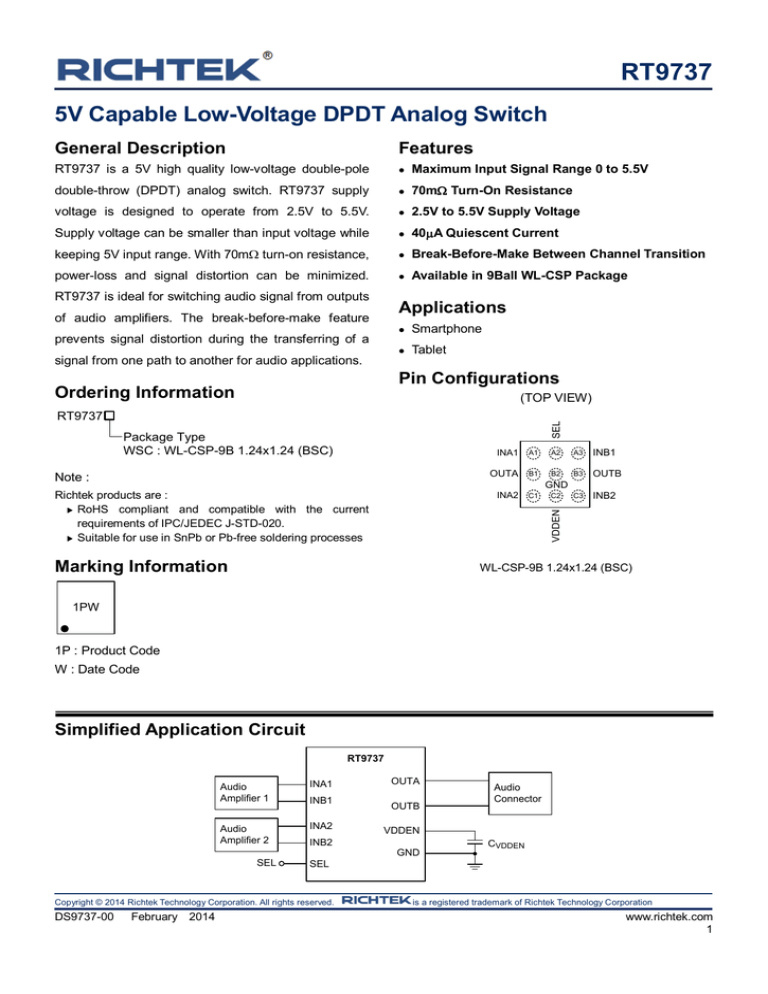
RT9737 is ideal for switching audio signal from outputs
Applications
of audio amplifiers. The break-before-make feature
Smartphone
Tablet
prevents signal distortion during the transferring of a
signal from one path to another for audio applications.
Pin Configurations
Ordering Information
(TOP VIEW)
SEL
RT9737
Package Type
WSC : WL-CSP-9B 1.24x1.24 (BSC)
Note :
INA1
A1
OUTA
B1
A2
A3
INB1
B2
B3
OUTB
C3
INB2
GND
Richtek products are :
RoHS compliant and compatible with the current
requirements of IPC/JEDEC J-STD-020.
Suitable for use in SnPb or Pb-free soldering processes
C1
C2
VDDEN
INA2
Marking Information
WL-CSP-9B 1.24x1.24 (BSC)
1PW
1P : Product Code
W : Date Code
Simplified Application Circuit
RT9737
Audio
Amplifier 1
INA1
Audio
Amplifier 2
INA2
INB1
OUTA
OUTB
VDDEN
INB2
GND
SEL
February 2014
CVDDEN
SEL
Copyright © 2014 Richtek Technology Corporation. All rights reserved.
DS9737-00
Audio
Connector
is a registered trademark of Richtek Technology Corporation
www.richtek.com
1
RT9737
Functional Pin Description
Pin No.
Pin Name
Pin Function
A1
INA1
Input 1 of Channel A.
A2
SEL
Selection for Input 1or 2.
A3
INB1
Input 1 of Channel B.
B1
OUTA
Output of Channel A.
B2
GND
Ground.
B3
OUTB
Output of Channel B.
C1
INA2
Input 2 of Channel A.
C2
VDDEN
Supply Voltage.
C3
INB2
Input 2 of Channel B.
Function Block Diagram
INA1
OUTA
INB1
INA2
OUTB
INB2
VDDEN
GND
SEL
Operation
The switches are fully specified to operate from a
via INA1 and INB1 to IC OUTA and OUTB. And then
single 2.5V to 5.5V power supply. RT9737 via internal
OUTA, OUTB output to the load and Audio connector.
design, be able to handle when the input signal is
When SEL voltage above high level, internal switch is
greater than the supply voltage range and don't cause
thrown to position 2. When the supply voltage VDDEN
the signal distortion. RT9737 control the switches with
under operation range, the switches impedance are
a control pin, SEL. When SEL voltage under low level,
risen and all analog signal ports can keep out signals
internal switch is thrown to position 1. Audio signal are
from 0V to 5.5V.
Copyright © 2014 Richtek Technology Corporation. All rights reserved.
www.richtek.com
2
is a registered trademark of Richtek Technology Corporation
DS9737-00
February 2014
RT9737
Absolute Maximum Ratings
(Note 1)
VDDEN, INA1, INA2, INB1, INB2, OUTA, OUTB, SEL------------------------------------------------- 0.3 to 6V
Power Dissipation, PD @ TA = 25C
WL-CSP-9B 1.24x1.24 (BSC)-------------------------------------------------------------------------------- 1.28W
Package Thermal Resistance
(Note 2)
WL-CSP-9B 1.24x1.24 (BSC), JA ------------------------------------------------------------------------ 78.1°C/W
Lead Temperature (Soldering, 10 sec.) ------------------------------------------------------------------- 260C
Junction Temperature ----------------------------------------------------------------------------------------- 150C
Storage Temperature Range -------------------------------------------------------------------------------- 65C to 150C
ESD Susceptibility
(Note 3)
HBM (Human Body Model) ----------------------------------------------------------------------------------- 2kV
MM (Machine Model) ------------------------------------------------------------------------------------------- 200V
Recommended Operating Conditions
(Note 4)
Supply Input Voltage, VDDEN-------------------------------------------------------------------------------- 2.5V to 5.5V
Junction Temperature Range --------------------------------------------------------------------------------- 40C to 125C
Ambient Temperature Range --------------------------------------------------------------------------------- 40C to 85C
Electrical Characteristics
(VDDEN = 2.5V, CVDDEN = 0.1μF, TA= 25C, for each LDO unless otherwise specified)
Parameter
Test Conditions
Symbol
Min
Typ Max Unit
Power Supply
Power Supply Range
VDDEN
2.5
--
5.5
V
--
80
--
dB
--
40
60
A
0
--
5.5
V
VDDEN = 2.5V, OUT = 0V, IOUT =100mA
--
90
125
m
VDDEN = 3.6V, OUT = 0V, IOUT= 100mA
--
70
100
m
INA, INB, OUTA, OUTB, VDDEN = 5.5V
--
1.2
1.5
A
0.12
0.2
A
--
5
10
ms
--
--
100
s
Power Supply Rejection Ratio PSRR
Vp-p = 200mV, f = 20kHz, RL = 32
Quiescent Current
VDDEN = 2.5V to 5.5V
IQ
(Note 5)
Analog Switch
Input Signal Range
Turn-On Resistance
RDS(ON)
Off-State Leakage Current
INA, INB, OUTA, OUTB = 5.5V, VDDEN = 0V
Turn-On Time
tON
INA, INB = 0V
Turn-Off Time
tOFF
INA, INB = 0V
Break-Before-Make Time
tBBM
INA, INB = 0V
VDDEN = 0V, RL = 50, INA/INB = 0.5Vpp,
20kHz
RL = 50, INA/INB = 0.5Vpp, 20kHz
RL = 50, INA/INB = 0.5Vpp, 1kHz, DC bias =
0.25V
RL = 50
--
5
10
ms
--
50
--
dB
--
80
--
dB
--
0.001
--
%
--
2
--
MHz
INA/INB Capacitance
INA /INB = 0.5VP-P, f = 1MHz (Note 5)
--
70
--
pF
OUTA/OUTB Capacitance
INA /INB = 0.5VP-P, f = 1MHz (Note 5)
--
120
--
pF
Off-Isolation
Crosstalk
THD+N
(Note 5)
(Note 5)
(Note 5)
-3dB Bandwidth
(Note 5)
Copyright © 2014 Richtek Technology Corporation. All rights reserved.
DS9737-00
February 2014
(Note 5)
is a registered trademark of Richtek Technology Corporation
www.richtek.com
3
RT9737
Parameter
Test Conditions
Symbol
Min
Typ Max Unit
Digital I/O
Input Logic-Hi Threshold
VIH
1.4
--
--
V
Input Logic-Low Threshold
VIL
--
--
0.4
V
0.1
--
0.1
A
Input Leakage Current
SEL = 0V or VDDEN
Note 1. Stresses beyond those listed “Absolute Maximum Ratings” may cause permanent damage to the device. These are
stress ratings only, and functional operation of the device at these or any other conditions beyond those indicated in the
operational sections of the specifications is not implied. Exposure to absolute maximum rating conditions may affect
device reliability.
Note 2. JA is measured at TA = 25C on a high effective thermal conductivity four-layer test board per JEDEC 51-7.
Note 3. Devices are ESD sensitive. Handling precaution is recommended.
Note 4. The device is not guaranteed to function outside its operating conditions.
Note 5. Guarantee by design.
Typical Application Circuit
RT9737
Audio
Amplifier 1
Audio
Amplifier 2
A1 INA1
A3 INB1
OUTB
B1
B3
INA2
C3 INB2
SEL
Copyright © 2014 Richtek Technology Corporation. All rights reserved.
Audio
Connector
2.5 to 5.5V
C1
A2
www.richtek.com
4
OUTA
VDDEN
C2
GND B2
CVDDEN
0.1μF
is a registered trademark of Richtek Technology Corporation
DS9737-00
February 2014
RT9737
Typical Operating Characteristics
Copyright © 2014 Richtek Technology Corporation. All rights reserved.
DS9737-00
February 2014
is a registered trademark of Richtek Technology Corporation
www.richtek.com
5
RT9737
Application Information
RT9737 is a 5V high quality low-voltage double-pole
a standard JEDEC 51-7 four-layer thermal test board.
double-throw (DPDT) analog switch. RT9737 supply
The maximum power dissipation at TA = 25C can be
voltage is designed to operate from 2.5 to 5.5V. Supply
calculated by the following formula :
voltage can be smaller than input voltage while keeping
PD(MAX) = (125C 25C) / (78.1C/W) = 1.28W for
5V input range. With 70m turn-on resistance, power-
WL-CSP-9B 1.24x1.24 (BSC) package
loss and signal distortion can be minimized. RT9737 is
The maximum power dissipation depends on the
ideal for switching audio signal from outputs of audio
operating ambient temperature for fixed TJ(MAX) and
amplifiers. The break-before-make feature prevents
thermal resistance, JA. The derating curve in Figure 1
signal distortion during the transferring of a signal from
allows the designer to see the effect of rising ambient
one path to another for audio applications.
temperature on the maximum power dissipation.
Analog Input
RT9737 internal topology design for input and output
Four-Layer PCB
voltage level can greater than supply voltage.
Low turn-on resistance and excellent channel to
channel matching are ideal for audio applications.
Switch Logic Control
RT9737 can use SEL pin to control internal switches
position for another audio source application. SEL pin
input current is very low.
Thermal Considerations
For continuous operation, do not exceed absolute
maximum junction temperature. The maximum power
Figure 1. Derating Curve of Maximum Power
Dissipation
dissipation depends on the thermal resistance of the IC
package, PCB layout, rate of surrounding airflow, and
The maximum power dissipation can be calculated by
the following formula :
OUTA
B1
A2
A3
B2
B3
ambient thermal resistance.
For recommended operating condition specifications,
the maximum junction temperature is 125C. The
junction to ambient thermal resistance, JA, is layout
1.24x1.24
C1
C2
C3
INB1
Use blind hole to
connect other strong
OUTB ground plane.
INB2
VDDEN
TA is the ambient temperature, and JA is the junction to
WL-CSP-9B
A1
INA2
where TJ(MAX) is the maximum junction temperature,
For
INA1
GND
PD(MAX) = (TJ(MAX) TA) / JA
dependent.
SEL
difference between junction and ambient temperature.
GND
CVDDEN
Place the capacitor CVDDEN as
close as possible to the VDDEN.
Figure 2. PCB Layout Guide
(BSC)
packages, the thermal resistance, JA, is 78.1C/W on
Copyright © 2014 Richtek Technology Corporation. All rights reserved.
www.richtek.com
6
is a registered trademark of Richtek Technology Corporation
DS9737-00
February 2014
RT9737
Preliminary
Outline Dimension
Dimensions In Millimeters
Symbol
Dimensions In Inches
Min.
Max.
Min.
Max.
A
0.500
0.600
0.020
0.024
A1
0.170
0.230
0.007
0.009
b
0.240
0.300
0.009
0.012
D
1.190
1.290
0.047
0.051
D1
E
0.800
1.190
0.031
1.290
0.047
0.051
E1
0.800
0.031
e
0.400
0.016
WL-CSP-9B 1.24x1.24 (BSC) Package
Richtek Technology Corporation
14F, No. 8, Tai Yuen 1st Street, Chupei City
Hsinchu, Taiwan, R.O.C.
Tel: (8863)5526789
Richtek products are sold by description only. Richtek reserves the right to change the circuitry and/or specifications without notice at any time. Customers should
obtain the latest relevant information and data sheets before placing orders and should verify that such information is current and complete. Richtek cannot assume
responsibility for use of any circuitry other than circuitry entirely embodied in a Richtek product. Information furnished by Richtek is believed to be accurate and
reliable. However, no responsibility is assumed by Richtek or its subsidiaries for its use; nor for any infringements of patents or other rights of third parties which may
result from its use. No license is granted by implication or otherwise under any patent or patent rights of Richtek or its subsidiaries.
Copyright © 2014 Richtek Technology Corporation. All rights reserved.
DS9737-00
February 2014
is a registered trademark of Richtek Technology Corporation
www.richtek.com
7


