Ultra Low Capacitance Diode Arrays Series
advertisement

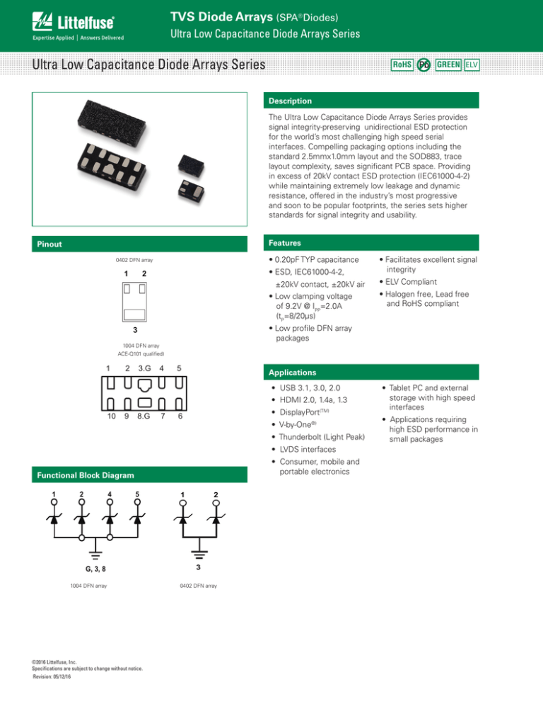
TVS Diode Arrays (SPA® Diodes) Ultra Low Capacitance Diode Arrays Series Ultra Low Capacitance Diode Arrays Series RoHS Pb GREEN ELV Description The Ultra Low Capacitance Diode Arrays Series provides signal integrity-preserving unidirectional ESD protection for the world’s most challenging high speed serial interfaces. Compelling packaging options including the standard 2.5mmx1.0mm layout and the SOD883, trace layout complexity, saves significant PCB space. Providing in excess of 20kV contact ESD protection (IEC61000-4-2) while maintaining extremely low leakage and dynamic resistance, offered in the industry’s most progressive and soon to be popular footprints, the series sets higher standards for signal integrity and usability. Features Pinout • 0.20pF TYP capacitance 0402 DFN array 1 2 • ESD, IEC61000-4-2, 3±20kV contact, ±20kV air 4 1 3 G 2 1004 DFN array ACE-Q101 qualified) 1 2 3.G 4 5 3 2 • Low clamping voltage of 9.2V @ IPP=2.0A (tP=8/20μs) 10 9 8.G 7 6 • Thunderbolt (Light Peak) • LVDS interfaces • C onsumer, mobile and portable electronics Functional Block Diagram 1 2 4 5 1 1004 DFN array 2 0402 DFN array 3 4 G ©2016 Littelfuse, Inc. Specifications are subject to change without notice. Revision: 05/12/16 2 3 G, 3, 8 1 (TM) • DisplayPort 6 • V-by-One®) Bottom View 5 6 • Halogen free, Lead free and RoHS compliant GApplications 1 • HDMI 2.0, 1.4a, 1.3 5 • ELV Compliant • Low profile DFN array packages • USB 3.1, 3.0, 2.0 4 • Facilitates excellent signal integrity • Tablet PC and external storage with high speed interfaces • Applications requiring high ESD performance in small packages TVS Diode Arrays (SPA® Diodes) Ultra Low Capacitance Diode Arrays Series Thermal Information Symbol Parameter Value Units IPP Peak Current (tp=8/20μs) 2.0 A Storage Temperature Range TOP Operating Temperature -30 to 85 °C °C Storage Temperature TSTOR -55 to 150 Parameter Rating Units -55 to 150 °C Maximum Junction Temperature 150 °C Maximum Lead Temperature (Soldering 20-40s) 260 °C SP1013 Absolute Maximum Ratings CAUTION: Stresses above those listed in “Absolute Maximum Ratings” may cause permanent damage to the device. This is a stress only rating and operation of the device at these or any other conditions above those indicated in the operational sections of this specification is not implied. Electrical Characteristics - (TOP=25°C) Typ Max Units Input Capacitance Parameter @ VR = 0V, f = 3GHz Test Conditions Min 0.20 0.22 pF Breakdown Voltage VBR @ IT=1mA 9.00 V Reverse Working Voltage Reverse Leakage Current IL @ VRWM=5.0V 25 Clamping Voltage VCL @ IPP=2.0A 9.20 ESD Withstand Voltage 50 nA 2.0 IEC61000-4-2 (Contact) ±20 IEC61000-4-2 (Air) ±20 Insertion Loss Diagram V V tP=8/20μs Peak Pulse Current 7.0 A kV Device IV Curve 1.0 0 0.8 0.6 0.4 -10.0 Current (mA) S21 Insertion Loss (dB) -5.0 -15.0 -20.0 0.2 0.0 -0.2 -0.4 -0.6 -25.0 -0.8 -30.0 1.E+06 -1.0 1.E+07 1.E+08 Frequency (Hz) 1.E+09 1.E+10 -2 -1 0 1 2 3 4 5 6 7 8 9 10 Voltage (V) ©2016 Littelfuse, Inc. Specifications are subject to change without notice. Revision: 05/12/16 TVS Diode Arrays (SPA® Diodes) Ultra Low Capacitance Diode Arrays Series USB3.0 Eye Diagram 5.0 Gb/s, 1000mV differential, CPO Compliant Test Pattern Without Device With Device Soldering Parameters Pre Heat Pb – Free assembly - Temperature Min (Ts(min)) 150°C - Temperature Max (Ts(max)) 200°C - Time (min to max) (ts) 60 – 180 secs Average ramp up rate (Liquidus) Temp (TL) to peak 3°C/second max TS(max) to TL - Ramp-up Rate 3°C/second max Reflow - Temperature (TL) (Liquidus) 217°C - Temperature (tL) 60 – 150 seconds tP TP Temperature Reflow Condition Critical Zone TL to TP Ramp-up TL TS(max) tL Ramp-do Ramp-down Preheat TS(min) 25 tS time to peak temperature Time Peak Temperature (TP) 260+0/-5 °C Time within 5°C of actual peak Temperature (tp) 20 – 40 seconds Lead Plating Pre-Plated Frame Ramp-down Rate 6°C/second max Lead Material Copper Alloy Time 25°C to peak Temperature (TP) 8 minutes Max. Lead Coplanarity 0.004 inches(0.102mm) Do not exceed 260°C Substrate material Silicon Body Material Molded Epoxy Flammability UL 94 V-0 Product Characteristics of 0402 DFN Package Part Numbering System SP xxxx U – ULC – 02 X T G TVS Diode Arrays (SPA® Diodes) G= Green T= Tape & Reel Size 1004 0402 Directional U: Unidirectional Ultra LC Package U: 1004 DFN E: 0402 DFN Notes : 1. All dimensions are in millimeters 2. Dimensions include solder plating. 3. Dimensions are exclusive of mold flash & metal burr. 4. Blo is facing up for mold and facing down for trim/form, i.e. reverse trim/form. 5. Package surface matte finish VDI 11-13. C Part Marking System Number of Channels C 0402 Ordering Information 4C Part Number Package Marking Reel Quantity SP0402U-ULC-02ETG 0402 DFN Array I C 10000 SP1004U-ULC-04UTG 1004 DFN Array I 4C 3000 ©2016 Littelfuse, Inc. Specifications are subject to change without notice. Revision: 05/12/16 MC MC 4C 1004 6C 6C TVS Diode Arrays (SPA® Diodes) Package Dimensions — 0402 DFN Array TOP VIEW END VIEW-1 SIDE VIEW-1 SIDE VIEW-2 Millimeters Symbol END VIEW-1 Min Typ Max Min Typ Max 0.33 - 0.55 0.013 0.015 0.022 A1 0 - 0.05 0 - 0.002 END VIEW-2 BOTTOM VIEW-1 SIDE VIEW-1 Inches A A3 TOP VIEW END VIEW-2 SIDE VIEW-2 0.13REF 0.25 0.005REF b 0.20 0.30 0.008 0.010 0.012 b’ 0.20 BOTTOM 0.30 VIEW-2 0.40 0.008 0.012 0.016 D 0.95 1.00 1.05 0.037 0.039 0.041 E 0.55 0.60 0.65 0.022 0.024 0.026 e 0.65BSC 0.026BSC e’ 0.675BSC 0.027BSC L 0.40 0.50 0.60 0.016 0.020 0.024 L1 0.10 0.15 0.20 0.004 0.006 0.008 SOLDERING PATTERN BOTTOM VIEW-2 BOTTOM VIEW-1 Embossed Carrier Tape & Reel Specification — 0402 DFN Array P1 SOLDERING PATTERN P2 P0 D0 E1 F W D1 Symbol Millimeters A0 0.70+/-0.05 B0 1.15+/-0.05 D0 ø 1.50+/-0.10 D1 ø 0.40 +/-0.10 E1 1.75+/-0.10 F 3.50+/-0.10 K0 0.55+/-0.05 P0 4.00+/-0.10 P1 2.00+/-0.10 P2 2.00+/-0.05 W 8.00+0.30/-0.10 T 0.20+/-0.05 T A0 K0 B0 ©2016 Littelfuse, Inc. Specifications are subject to change without notice. Revision: 05/12/16 SP1013 Ultra Low Capacitance Diode Arrays Series TVS Diode Arrays (SPA® Diodes) Ultra Low Capacitance Diode Arrays Series Package Dimensions — 1004 DFN Array Symbol BOTTOM VIEW-1 BOTTOM VIEW-2 SIDE VIEW-2 SIDE VIEW-1 BOTTOM VIEW-3 SOLDERING PATTERN A 0.33 0.43 0.013 0.017 A' 0.50 0.60 0.020 0.024 A'' 0.45 0.55 0.018 0.022 A1 0.00 0.05 0.000 0.002 ALTERNATIVE UNIT: mm Max A3 0.127 ref. 0.005 ref. 0.15 ref. 0.006 ref. 0.15 0.25 0.006 0.010 b2 0.35 0.45 0.014 0.018 b3 0.20 0.30 0.008 0.012 D 2.40 2.60 0.094 0.102 E 0.90 1.10 0.035 0.043 L RECOMMENDED Min A3' e TOP VIEW Inches Max b1 SIDE VIEW-3 Millimeters Min 0.50 BSC 0.020 BSC 0.28 0.48 0.011 0.019 L' 0.35 0.45 0.014 0.018 L1 0.00 0.15 0 L2 0.05 REF 0.002 REF L3 0.075 REF 0.003 REF R R' 0.125 REF 0.05 0.005 REF 0.15 0.002 0.006 Embossed Carrier Tape & Reel Specification — 1004 DFN Array D0 T Y P0 P2 E1 D1 F B0 K0 Section Y - Y A0 ©2016 Littelfuse, Inc. Specifications are subject to change without notice. Revision: 05/12/16 Y P1 W Symbol Millimeters A0 1.15 min/1.30 max B0 2.70+/-0.05 D0 ø 1.50 min/1.65 max D1 ø 0.50 min/1.05 max E1 1.75+/-0.10 F 3.50+/-0.10 K0 0.46 min/0.75 max P0 4.00+/-0.10 P1 4.00+/-0.10 P2 2.00+/-0.05 W 8.00+0.30/-0.10 T 0.17 min/0.30 max


