APPLICATION NOTE
UNDERSTANDING POWER FACTOR
by L. Wuidart
IF YOU THINK THAT POWER FACTOR IS
ONLY COS ϕ, THINK AGAIN !
The big majority of Electronics designers do not
worry about Power Factor (P.F.)
P.F. is something you learnt one day at school in
your Electrotechnics course"as being cos ϕ.
This conventional definition is only valid when
considering IDEAL Sinusoidal signals for both
current and voltage waveforms.
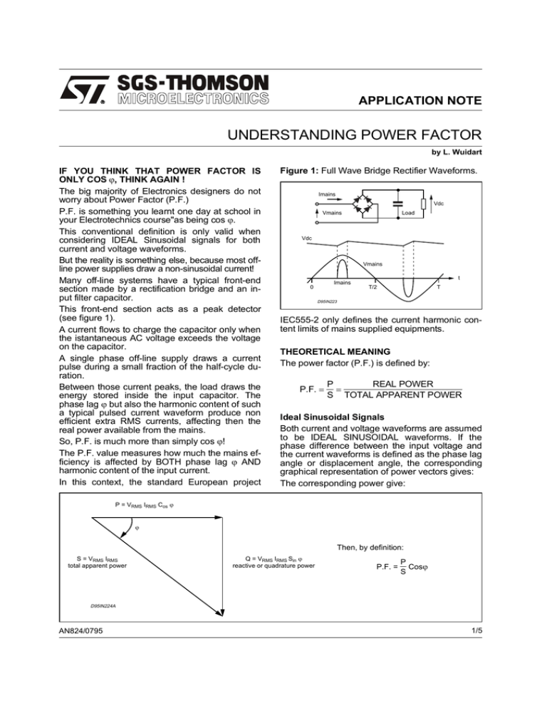
But the reality is something else, because most offline power supplies draw a non-sinusoidal current!
Many off-line systems have a typical front-end
section made by a rectification bridge and an input filter capacitor.
This front-end section acts as a peak detector
(see figure 1).
A current flows to charge the capacitor only when
the istantaneous AC voltage exceeds the voltage
on the capacitor.
A single phase off-line supply draws a current
pulse during a small fraction of the half-cycle duration.
Between those current peaks, the load draws the
energy stored inside the input capacitor. The
phase lag ϕ but also the harmonic content of such
a typical pulsed current waveform produce non
efficient extra RMS currents, affecting then the
real power available from the mains.
So, P.F. is much more than simply cos ϕ!
The P.F. value measures how much the mains efficiency is affected by BOTH phase lag ϕ AND
harmonic content of the input current.
In this context, the standard European project
Figure 1: Full Wave Bridge Rectifier Waveforms.
Imains
Vdc
Vmains
Load
Vdc
Vmains
Imains
0
t
T/2
T
D95IN223
IEC555-2 only defines the current harmonic content limits of mains supplied equipments.
THEORETICAL MEANING
The power factor (P.F.) is defined by:
P.F. =
REAL POWER
P
=
S TOTAL APPARENT POWER
Ideal Sinusoidal Signals
Both current and voltage waveforms are assumed
to be IDEAL SINUSOIDAL waveforms. If the
phase difference between the input voltage and
the current waveforms is defined as the phase lag
angle or displacement angle, the corresponding
graphical representation of power vectors gives:
The corresponding power give:
P = VRMS IRMS Cos ϕ
ϕ
Then, by definition:
S = VRMS IRMS
total apparent power
Q = VRMS IRMS Sin ϕ
reactive or quadrature power
P.F. =
P
Cosϕ
S
D95IN224A
AN824/0795
1/5
APPLICATION NOTE
As ϕ1 is the displacement angle between the input voltage and the in-phase component of the
fundamental current:
Non-ideal sinusoidal current waveform
Assume that the mains voltage is an IDEAL
SINUSOIDAL voltage waveform.
Its RMS value is:
VRMS =
I1RMS P = I1RMS Cosϕ1
Vpeak
2
√
and
P = VRMS ⋅ I1RMS ⋅ Cosϕ1
S = VRMS ⋅ IRMS total
If the current has a periodic non-ideal sinusoidal
waveform, the FOURIER transform can be applied
Then, the Power Factor can be calculated as:
IRMS total = √
I2O + I2 1RMS + I2 2RMS +....+ I2 nRMS
P.F. =
Where IO is the DC component of the current,
I1rms the fundamental of the RMS current and
I2RMS ....InRMS the harmonics
For a pure AC signal:
One can introduce the k factor by
IO = 0
k=
The fundamental of the RMS current has an inphase component I1RMSP and a quadrature component I1RMSQ.
So, the RMS current can be espressed as:
IRMS total =
√
I
P+I
Q+∑ I
2
1RMS
2
1RMS
I1RMS
IRMS total
= CosΘ
Θ is the distortion angle. The k factor is linked to
the harmonic content of the current. If the harmonic content of IRMS total is approaching zero,
k------> 1.
∞
2
P I1RMS ⋅ Cosϕ1
=
S
IRMS total
nRMS
Conclusion
Finally P.F. can be expressed by:
P.F. = CosΘ ⋅ Cos ϕ1
So, the power vectors representation becomes
n=2
Then, the Real Power is given by:
P = VRMS ⋅ I1RMS P
In-phase
P = Real Power = VRMS · I1RMS Cos ϕ1
ϕ1
S
ot
al
= VRMS · I1RMS Sin ϕ1
are
nt fu
nda
=V
m
θ
-T
Q = Reactive Power
S1 =
App
· I1
MR
S
ap
enta
RM
pa
S
re
nt
quadrature
l po
wer
Po
we
r-
V
RM
S
·I
RM
S
to
ta
l
D = Distortion Power
= VRMS
√ ∑∞n=2 I2nRMS
D95IN225A
ϕ1 is the "conventional" displacement angle (phase lag) between the in-phase fundamental I and V
Θ is the distortion angle linked to the harmonic content of the current.
Both of reactive (Q) and distortion (D) powers produce extra RMS currents, giving extra losses so that then the
mains supply network efficiency is decreased.
Improving P.F. means to improve both of factors i.e.:
ϕ1 → 0 ⇒ Cos ϕ1 → 1 ⇒ reduce phase lag between I and V
Θ → 0 ⇒ Cos Θ → 1 ⇒ reduce harmonic content of I
2/5
APPLICATION NOTE
PRACTICAL MEANING
The unity power factor beneficiaries
Both of the user and the Electricity distribution
company take advantage from a unity power factor. Moreover, adding a PFC brings components
cost reduction in the downstream converter.
The user’s benefit
At minimum line voltage (85VAC), a standard
115VAC well socket should be able to deliver the
nominal 15A to a common load.
In similar conditions, a "non-corrected power factor" SMPS (typical value of 0.6) drops the available current from 15A to only 9A.
For example, from one wall socket, four 280W
computers each equipped with P.F.C. can be
supplied instead of two with no P.F.C.
The Electricity distribution company benefit
Both of reactive (Q) power and distortion (D)
power produce extra RMS currents.
The resulting extra losses significantly decrease
the mains supply network efficiency. This leads to
oversize the copper area of distribution power
wires (see figure 3)
The distortion power is linked to the current harmonic content. Delivering power at other frequencies than the line frequency causes a lot of drawbacks.
The current distortion disturbs the zero crossing
detection systems, generates overcurrent in the
neutral line and resonant overvoltages.
In Europe, the standard EN 60555 and the international project IEC 555-2 limit the current harmonic content of mains supplied equipments.
Figure 2: Reactive and distortion power produce extra RMS currents leading to copper area oversize.
Without P.F.C.
115VAC/15A
With P.F.C.
D95IN227
Figure 3: Reactive and distortion power produce extra RMS currents leading to copper area oversize.
3/5
APPLICATION NOTE
Components cost reduction in the downstream converter
For the same output power capability, a conventional converter using a input mains voltage doubler, is penalized by a 1,8 times higher primary
RMS current than with a PFC preregulator.
Consequently, the PFC allows to select power
MOSFET’s switches with up to 3 times higher on
resistance (rds on) in the downstream converter
(see figure 4).
The converter transformer size can be optimized
not only because the copper area is smaller but
also, due to the regulated DC bulk voltage delivFigure 4: Power MOSFET On-resistance (rds on)
is 3 times higher by using a PFC.
without P.F.C.
rds on
with P.F.C.
rds onX3
ered by the PFC preregulator.
The PFC provides an automatic mains selection
on a widerange voltage from 85VAC up to
265VAC. Compared to the conventional doubler
front-end section, the same "hold-up" time can be
achieved with a 6 times smaller bulk storage capacitor.
To get 10ms hold-up time, a 100W converter in
doubler operation requires a series combination
of two 440µF capacitos instead of one 130µF with
PFC.
General comments
For new developments, SMPS designers will
have to consider the IEC 555-2 standard.
In the practice, this leads to use a PFC is compensated by significant component cost reduction
in the downstream converter.
The PFC also provides additional functions such
as automatic mains voltage selection and a constant output voltage.
Nevertheless, size a nd cost optimization of PFC
has to take the RFI filter section into account.
A PFC circuit generates more high frequency interferences to the mains than a conventional rectifier front-end section (see figure 5).
The PFC use requires thus additional filtering. For
this reason, modulation techniques and mode of
operation for the PFC have to be carefully
adapted to the application requirement.
Figure 5: A Power Factor Converter generates higher frequency interferences to the mains than a
conventional rectifier front-end
lower sym.
attenuation filter
Ci
220µF
Usaual SMPS structure
higher sym.
attenuation filter
Ci
0.1µF
P.F.C. structure
D95IN226
4/5
APPLICATION NOTE
Information furnished is believed to be accurate and reliable. However, SGS-THOMSON Microelectronics assumes no responsibility for the
consequences of use of such information nor for any infringement of patents or other rights of third parties which may result from its use. No
license is granted by implication or otherwise under any patent or patent rights of SGS-THOMSON Microelectronics. Specifications mentioned in this publication are subject to change without notice. This publication supersedes and replaces all information previously supplied.
SGS-THOMSON Microelectronics products are not authorized for use as critical components in life support devices or systems without express written approval of SGS-THOMSON Microelectronics.
© 1995 SGS-THOMSON Microelectronics - All Rights Reserved
SGS-THOMSON Microelectronics GROUP OF COMPANIES
Australia - Brazil - France - Germany - Hong Kong - Italy - Japan - Korea - Malaysia - Malta - Morocco - The Netherlands - Singapore Spain - Sweden - Switzerland - Taiwan - Thaliand - United Kingdom - U.S.A.
5/5


