Thin Solid Films 534 (2013) 348–355
Contents lists available at SciVerse ScienceDirect
Thin Solid Films
journal homepage: www.elsevier.com/locate/tsf
Detailed analysis of defect reduction in electrowetting dielectrics through a two-layer
‘barrier’ approach
A. Schultz a, S. Chevalliot a, b, S. Kuiper c, J. Heikenfeld a,⁎
a
b
c
School of Electronic and Computing Systems, Novel Devices Laboratory, The University of Cincinnati, Cincinnati, OH, 45221, USA
Varioptic, 24B rue Jean Baldassini, 69007 Lyon - France
Optilux Inc., 1735 East Bayshore Road, Unit 8B Redwood City, CA 94063, USA
a r t i c l e
i n f o
Article history:
Received 27 August 2012
Received in revised form 27 February 2013
Accepted 1 March 2013
Available online 20 March 2013
Keywords:
Electrowetting
Dielectric
Interfacial tension
Parylene
a b s t r a c t
Low-voltage electrowetting requires a thin dielectric capacitor and field strengths approaching 1 MV/cm. Unlike
traditional metal/dielectric/metal capacitors, the conducting electrowetted liquid can electrically propagate
through the smallest dielectric defects or pores, even for the best barrier polymers such as Parylenes, leading
to catastrophic failure such as electrolysis. A detailed analysis of double layer dielectric systems is shown to provide >100 times reduction in defect density, with >10 cm2 area exhibiting no dielectric failure at >2 times the
required electrowetting voltage. An anodized-Al2O3/Parylene-HT stack provides electrowetting contact angle
modulation down to saturation at 70° at b15 V with breakdown protection to >3 times that voltage. These
results build on previous findings on the effect of ion type, liquid type, polymer dielectric choice, electrode
material, and provide a next major advance in electrowetting reliability.
© 2013 Elsevier B.V. All rights reserved.
1. Introduction
Electrowetting [1] is well known for its use in applications ranging
from optics [2–4], to displays [5,6], to lab-on-chip [7–9]. Reliable
electrowetting is commercially proven, a prime example being the
Varioptic Artic 316 ‘liquid lens’ product which provides >10 8
switching cycles with a several μm-thick Parylene dielectric and 60
VRMS operation. Low-voltage (b15 V) operation has also been demonstrated by several research groups using higher capacitance dielectrics,
as recently reviewed by Liu et al. [10]. However, largely unpublished are
the very short operating lifetimes (minutes) and low fabrication yields
(>1 catastrophic defect/cm 2) for such attempts. Device degradation
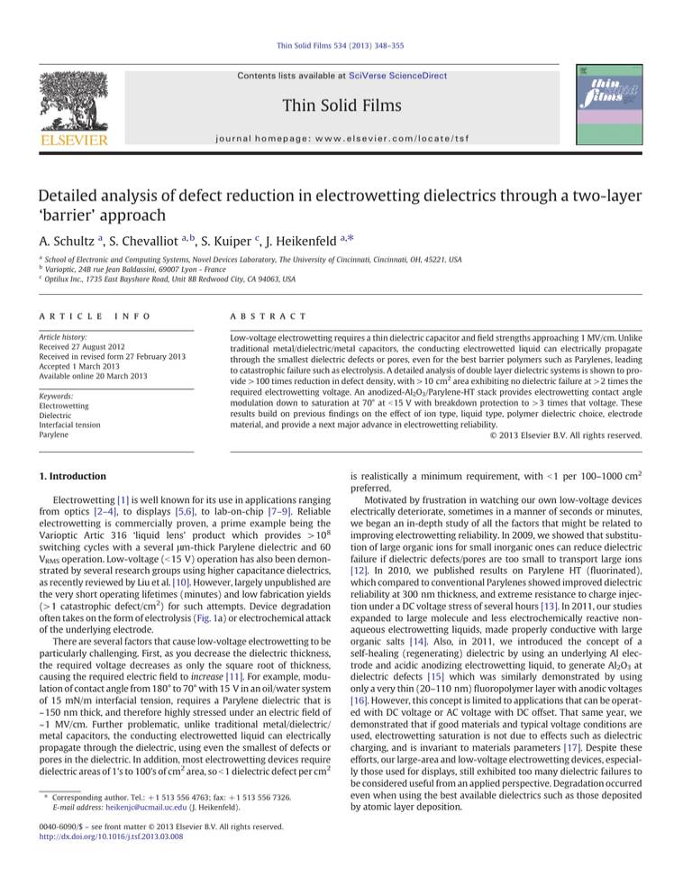
often takes on the form of electrolysis (Fig. 1a) or electrochemical attack
of the underlying electrode.
There are several factors that cause low-voltage electrowetting to be
particularly challenging. First, as you decrease the dielectric thickness,
the required voltage decreases as only the square root of thickness,
causing the required electric field to increase [11]. For example, modulation of contact angle from 180° to 70° with 15 V in an oil/water system
of 15 mN/m interfacial tension, requires a Parylene dielectric that is
~150 nm thick, and therefore highly stressed under an electric field of
~1 MV/cm. Further problematic, unlike traditional metal/dielectric/
metal capacitors, the conducting electrowetted liquid can electrically
propagate through the dielectric, using even the smallest of defects or
pores in the dielectric. In addition, most electrowetting devices require
dielectric areas of 1's to 100's of cm2 area, so b 1 dielectric defect per cm2
⁎ Corresponding author. Tel.: +1 513 556 4763; fax: +1 513 556 7326.
E-mail address: heikenjc@ucmail.uc.edu (J. Heikenfeld).
0040-6090/$ – see front matter © 2013 Elsevier B.V. All rights reserved.
http://dx.doi.org/10.1016/j.tsf.2013.03.008
is realistically a minimum requirement, with b1 per 100–1000 cm2
preferred.
Motivated by frustration in watching our own low-voltage devices
electrically deteriorate, sometimes in a manner of seconds or minutes,
we began an in-depth study of all the factors that might be related to
improving electrowetting reliability. In 2009, we showed that substitution of large organic ions for small inorganic ones can reduce dielectric
failure if dielectric defects/pores are too small to transport large ions
[12]. In 2010, we published results on Parylene HT (fluorinated),
which compared to conventional Parylenes showed improved dielectric
reliability at 300 nm thickness, and extreme resistance to charge injection under a DC voltage stress of several hours [13]. In 2011, our studies
expanded to large molecule and less electrochemically reactive nonaqueous electrowetting liquids, made properly conductive with large
organic salts [14]. Also, in 2011, we introduced the concept of a
self-healing (regenerating) dielectric by using an underlying Al electrode and acidic anodizing electrowetting liquid, to generate Al2O3 at
dielectric defects [15] which was similarly demonstrated by using
only a very thin (20–110 nm) fluoropolymer layer with anodic voltages
[16]. However, this concept is limited to applications that can be operated with DC voltage or AC voltage with DC offset. That same year, we
demonstrated that if good materials and typical voltage conditions are
used, electrowetting saturation is not due to effects such as dielectric
charging, and is invariant to materials parameters [17]. Despite these
efforts, our large-area and low-voltage electrowetting devices, especially those used for displays, still exhibited too many dielectric failures to
be considered useful from an applied perspective. Degradation occurred
even when using the best available dielectrics such as those deposited
by atomic layer deposition.
A. Schultz et al. / Thin Solid Films 534 (2013) 348–355
349
Fig. 1. Diagrams and photos of (a) a failed single-layer electrowetting dielectric exhibiting electrolysis; (b) improved operation with a multi-layer dielectric that does not exhibit
dielectric failure.
An additional materials advance is clearly needed to reduce the
density of defects in electrowetting dielectrics, ideally using a fabrication approach that is both highly economical and deposited at or
near room-temperature. We report here a detailed analysis of significant defect reduction in electrowetting dielectrics through a simple
double-layer ‘Barrier’ approach. We observe >100 times reduction in
defect density compared to single layer dielectrics, with >10 cm2 area
exhibiting no dielectric failure at >2 times the operating voltage. A simple anodized Al2O3/Parylene-HT stack provides electrowetting contact
angle modulation down to 70° at b15 V with no dielectric failure at
up to >3 times that voltage. Although not the only investigation of
multi-layer electrowetting dielectrics [18,19], this expands on previous
investigations to address important issues such as defect density, and to
examine the materials requirements in detail. Furthermore, our experimental evidence suggests that the improved dielectric performance
may not be due to the organic dielectric filling or passivation of defects
in the underlying dielectric, as suggested by Lin et al. [18]. Rather, it
appears that the improvement is due to creating a tortuous path for
liquid/ion penetration (Fig. 1b), which is analogous to multi-layer
inorganic/organic gas/moisture barriers developed for encapsulation
of organic light emitting diode displays [20,21]. Our results provide a
significant advance and build on a large cumulative body of work
toward reliable low-voltage electrowetting.
2. Experimental methods
Electrowetting tests were performed using simple sessile droplet
tests similar to that shown in Fig. 1. Sodium dodecyl sulfate (SDS) was
added to de-ionized water to create the conducting test liquid. SDS is
well characterized in electrowetting systems and provides a mechanism to test the effect of ion-size on dielectric failure [12,13]. With positive voltage to the aqueous solution, the small sodium cations (Na+)
will be responsible for dielectric failure, whereas with negative voltage,
it is the large dodecyl sulfate anions. Although non-aqueous solutions
are preferred for improved reliability in displays or optics [14], aqueous
solution was tested because it is often required for some electrowetting
applications such as lab-on-chip (chemical properties) and liquid lenses
(optical properties). The oil tested was OS-30 silicone oil from Dow
Corning.
Two types of dielectric failure tests were performed. Small area
(~ 0.5 cm 2) tests were designed for investigating resistance to failure
due to the more homogeneous nature of the dielectric film (i.e. none
or few of the large-size defects). These tests were carried out in air using
a 0.7 μm Platinum probe and 1 μL, 0.01 wt.% SDS solution droplets.
These experiments are always performed in air (not insulating oil) because that makes the droplet less mobile due to contact angle hysteresis.
Without contact angle hysteresis, at higher voltages, inhomogeneous
charging of the dielectric can cause the droplet to spontaneously
leap away from the probe. DC voltage was applied at a slow step rate
of ±1 V/s up to ±98 V with the electrode under the dielectric grounded. This slow step rate is needed for electrowetting reliability testing because dielectric failure mechanisms typically evolve over time (e.g. are
not due to classical electrical breakdown). Five droplets per dielectric
sample were tested and the current was recorded every 1 volt. Dielectric
failure was attributed to current exceeding a value of ±1 μA.
A second, large area test, was implemented to capture dielectric failure due to large and inhomogeneous dielectric features (defects). The
same SDS solution was confined over an area of ~100 cm2 with use of a
polydimethysiloxane gasket and a glass plate with a transparent In2O3:
SnO2 bias electrode. The transparent top plate allowed photographic capture of breakdown, observed by bubble formation (electrolysis). For the
large area tests, a very slow ramp rate of 1 V/5 s was applied up to
30 V with the maximum current clamped to b10 mA. Top-view photos
were taken every 1 V and combined sequentially into a video [22]. Simultaneously, electrical current was measured to further quantify the magnitude of dielectric failure.
A large variety of single-layer and two-layer dielectrics were tested
in order to reveal what characteristics promote a reliable multi-layer dielectric (Table 1). For all experiments, borosilicate glass substrates were
first sputter-deposited with a ~400 nm Al electrode. Thicker Al was utilized in some experiments, so that an Al2O3 dielectric could be formed
by room-temperature anodization in an electrolytic ammonium phosphate solution (~2 wt.%, ~2 nm/V). Organic dielectrics were also tested,
including Parylene C (chlorinated) and Parylene HT (fluorinated). Both
350
A. Schultz et al. / Thin Solid Films 534 (2013) 348–355
Table 1
Tested single-layer and multi-layer dielectrics. The Cytop
fluoropolymer has little influence on electrowetting reliability (explained elsewhere in this paper) and is not
counted in the ‘single’ or ‘double’ nomenclature.
Single layer
150 nm Al2O3/50 nm Cytop
300 nm SU-8/50 nm Cytop
50 nm Parylene C/50 nm Cytop
50 nm Parylene HT/50 nm Cytop
Two layer
150 nm Al2O3/50 nm Parylene C/50 nm Cytop
150 nm Al2O3/50 nm Parylene HT/50 nm Cytop
300 nm SU-8/50 nm Parylene C/50 nm Cytop
300 nm SU-8/50 nm Parylene HT/50 nm Cytop
50 nm Parylene C/50 nm Parylene HT/50 nm Cytop
Parylene types were respectively deposited at room-temperature by
chemical vapor deposition in a Specialty Coating Systems PDS2010
or PDS2035CR lab coater. MicroChem's SU-8 2000 series negative
epoxy photoresist was also tested as a dielectric because it has been
reported to have very high breakdown field [23], possibly because it is
re-melted after spin-coating and solvent evaporation, and then crosslinked with UV exposure. The SU-8 and Parylenes were all processed
using their standard manufacturer-stated conditions. In addition, all
single-layer and multi-layer dielectric samples were spin coated with
50 nm Asahi Glass Cytop fluoropolymer using 1 wt.% Cytop 809 M
and baking at 180 °C for 30 min. This top fluoropolymer layer provides
hydrophobicity for a large Young's contact angle, but is not required if
an insulating liquid (oil) has an interfacial tension that properly
matches the top dielectric surface [13,24].
Before discussing the experimental results, there are two brief
but important topics to be discussed. First, the top fluoropolymer layer
is not counted toward preventing dielectric failure in any of the experiments. If placed on a second high-quality dielectric, the porosity of thin
fluoropolymers is adequately low to allow electrowetting. However,
when deposited at thicknesses (b100–200 nm) required for lowvoltage operation, we have observed that the porosity/defectivity for
all solution-deposited fluoropolymers (Cytop 809 M, Teflon AF 1600,
Fluoropel 1601 V, etc.) is too high to provide any meaningful improvement in the reliability of a stack of dielectrics. Furthermore, with
the correct choice of dielectric and insulating oil, no fluoropolymer is
needed [24]. A second topic relates to the choice of using anodically
grown Al2O3, which is inherently electrochemically porous by nature
of the anodization. It therefore is an ideal dielectric to investigate if
multi-layer dielectrics would provide any improvement to reliability.
We disagree with the conclusions of Lin et al., [18] who stated:
“Among the materials tested, the dielectric constants of Al2O3 and
Si3N4 are too low for practical use.” We will show that the comparatively low dielectric constants of Al2O3 and Si3N4 are suitable enough for
low-voltage electrowetting with a stacked electrowetting dielectric.
Furthermore, higher dielectric constant materials are often less electrochemically stable, need to be thicker (more strain, defects), exhibit
stronger charge trapping/hysteresis.
Lastly, we note that beyond Al electrode coating, all additional
fabrication processes were performed under the most challenging
case: a non-cleanroom environment without climate control. Both the
anodization and Parylene coating techniques are resilient to particulates and surface contamination, such that any reliable films achieved
should be easily reproduced by others.
with a low dielectric constant leads to field amplification in the layer
with the low constant. In practical situations, this often leads to breakdown of the latter. This was pointed out by Kuiper et al. [11] Previous
theoretical plots do not account for electrical breakdown limits, nor
do they account for how a defect in one layer can cause the entire
voltage drop to appear across the other layer [24,25]. The following
derivations provide suitable ranges within which the experiments
were performed.
The required voltage (V) can be derived from the electrowetting
equation [26]: cosθV = (γid – γcd)/γci + (C∙V2)/(2∙γci), (1), where C is
the dielectric capacitance and the γ terms are the interfacial tensions
between the conducting (c), insulating (i) liquid, and the dielectric
(d). Using simple series capacitor equations, two limiting cases can be
derived: no defects, Elayer = (V∙Ctot)/(Clayer∙dlayer), (2), and a defect in
layer 1, Elayer2 = V/dlayer2, (3), where each term with subscript ‘layer’
is the electric field (E), capacitance (C), or thickness (d) for that respective layer.
A challenging and practically relevant case will be chosen: γci =30
mN/m and electrowetting from (γid – γcd)/γci = − 1 (θ = 180º) to
θV = 70º. Fig. 2a plots the theoretical electric field across a 150 nm
Al2O3 layer and a Parylene HT layer as the Parylene HT thickness is
varied (Eq. 2, blue and red lines). The electric field across the Al2O3
layer is also plotted for the case of a defect in the Parylene HT layer
(Eq. 3, black line). Fig. 2b is similar, but Parylene HT is fixed at 100 nm
and instead, the Al2O3 thickness is varied. 2 MV/cm is assumed as the
breakdown field for both dielectrics with a liquid electrode, indicated
by the horizontal green line. Blue dotted lines represent a limiting window to avoid dielectric failure. Several key conclusions are as follows.
Firstly, if the Parylene HT layer is made too thick and has a defect in it,
the Al2O3 layer will experience the entire applied voltage at that defect.
3. Theoretical expectations
No dielectric stack is useful if the electrical field across any individual
layer in the stack exceeds its bulk electrical breakdown limit. Using an
insulator with a high dielectric constant in combination with a dielectric
Fig. 2. Plots of theoretical electric fields across the different dielectric layers vs. (a) Parylene
HT thickness with 150 nm Al2O3 and 50 nm Cytop with, and vs. (b) Al2O3 thickness with
100 nm Parylene HT and 50 nm Cytop.
A. Schultz et al. / Thin Solid Films 534 (2013) 348–355
This would likely cause the Al2O3 layer to exceed its breakdown field
and thereby causing complete dielectric failure (Fig. 2a). Secondly,
Al2O3 thickness is a less important factor. Thirdly, if the data were
replotted for γci = 50 mN/m (not shown), as is the case for some
lab-on-chip applications, there would be no reliable operating window!
These theoretical plots show that careful consideration of dielectric
thickness must be made if thin dielectrics are used to achieve
low-voltage operation. For further investigation, an Excel spreadsheet
is provided which calculates the electric fields across various layers,
with and without the presence of defects in any particular layer [22].
4. Experimental results
Theoretical investigations aided the selection of materials and
thicknesses listed in Table 1. The SU-8 was implemented thicker
than Parylene despite the high breakdown field of SU-8, because it
is generally difficult to make impermeable dielectrics by spin or dip
coating.
Fig. 3 plots small area droplet tests on the single-layer dielectrics
listed in Table 1. The polarity dependence of dielectric failure is consistent with our previous conclusions on self-healing by anodization [15],
and ion size (large dodecyl sulfate anion vs. small Na + [12]), with
more subtle effects possible due to Debye screening within pores or
defects. The most challenging test is positive bias (Na+), where all
dielectrics performed very poorly individually. Even if the dielectrics
performed well in negative bias due to anodization of the underlying
aluminum electrode, the results cannot be applied to all electrowetting
applications since DC (mono-polar) operation of electrowetting devices
can lead to long-term charging and ion migration. These results also
confirm our initial assumption that the Cytop layer does not significantly contribute to preventing breakdown with a liquid electrode (with a
351
solid electrode it should sustain ~10 V). With a clear indication that
these single-layer dielectrics were insufficient for reliable operation,
the experiments next turned to two-layer inorganic/organic dielectrics.
Figs. 4 and 5 plot small area droplet tests on Al2O3/Parylene and SU-8/
Parylene dielectric stacks, respectively. Only Parylene HT exhibited
the desired level of reliability. Although much thinner in this work,
our previous results have similarly shown that at 300 nm Parylene HT
is more reliable than Parylene C [13]. It must, however, be noted that
Parylene C was heated to 180 °C for 30 min, whereas the short-term
(24 h) service temperature is only 100 °C. It is not clear how this has
affected the performance of Parylene C. The short-term service temperature for Parylene HT is 450 °C, which makes it likely that its performance was not influenced by the 180 °C treatment. For the Al2O3/
Parylene HT (Fig. 4) and SU-8/Parylene HT (Fig. 5) results, the dielectric
failure occurs at ~65–70 V on average, which is ~2 times and ~4 times,
respectively, the sum of the voltages for failure for each dielectric individually (Fig. 3). It is clear that combining these dielectrics provides
an enhancement in reliability that none of these dielectrics has
individually.
The small ~0.5 cm2 area droplet tests of Figs. 3 and 4 clearly show
value of stacked dielectrics, particularly with Parylene HT top-layers.
These samples show resistance to failure due to the more homogeneous
nature of the dielectric stack. Next, 200 times larger area was tested to
assess dielectric failure due to larger and inhomogeneous dielectric
defects.
Fig. 6 shows brightness and contrast adjusted photographs of
dielectric failure for large-area samples (3.8×2.6 cm2). Ambient white
light was enough illumination to allow light scattering from gas bubbles
formed at major dielectric defects (electrolysis). It should be noted that
a defect generating the 1 μA of current for the plots in Figs. 3–5 does
not necessarily lead to gas bubble sizes large enough to visualize in
Fig. 3. Plots of current vs. voltage (1 V/s ramp) for (a) 150 nm Al2O3/50 nm Cytop, (b) 300 nm SU-8/50 nm Cytop, (c) 50 nm Parylene C/50 nm Cytop, and (d) 50 nm Parylene HT/50 nm
Cytop. The Al electrode was grounded and the test solution was 0.01 wt.% SDS in water surrounded by air.
352
A. Schultz et al. / Thin Solid Films 534 (2013) 348–355
Fig. 4. Plots of current vs. voltage (1 V/s ramp) for (a) 150 nm Al2O3/50 nm Parylene
C/50 nm Cytop, and (b) 150 nm Al2O3/50 nm Parylene HT/50 nm Cytop. The Al electrode
was grounded and the test solution was 0.01 wt.% SDS in water surrounded by air.
the photographs of Fig. 6. Therefore, the results of Fig. 6 should be
analyzed independently of the previous discussion and conclusions.
It is visually obvious that all of the single-layer dielectrics (Fig. 6a–c)
exhibit an intolerable density of major defects even at 10 V, which corresponds to electric fields below bulk breakdown fields in each layer for
every sample tested. An ideal goal would be that no defects should
cause dielectric failure for at least 2 times the targeted operation voltage
of b15 V. Fig. 6d-e are for the Al2O3/Parylene stacks which exhibited
very few major defects, if any at all for Al2O3/Parylene HT. For the
Al2O3/Parylene HT test, few points of light scattering existed at 0 V
and did not change with voltage, and therefore are just due to particulates (e.g. no dielectric failure). The number of gas bubbles present for
each 1 V step was counted using Image J software from every sample
shown in Fig. 6, and the data are plotted in Fig. 7. It should be noted
that the defect count above ~15 V for the single-layer cases were difficult to discern due to coalescence of larger bubbles and spreading
of small bubbles over the entire surface where there were no visible
defects. The complete absence of bubble generation for Al2O3/Parylene
HT, over a large area of ~100 cm2, for the challenging case of positive
voltage (small Na+) at 30 V and 150 s, and even up to 40 V and
200 s (not shown), is unlike any result we have previously observed
or seen reported for such a thin dielectric stack. Even the Al2O3/Parylene
C results are highly encouraging, and may prove valuable to those who
do not have access to Parylene HT coating capability.
It is obvious that the tested single-layer dielectrics do not electrically
compare to those of the stacked dielectrics when considering the capacitances. Therefore, for completeness of understanding, single-layer
Parylene HT large area samples with thicknesses chosen to match the
capacitance of the stacked Al2O3/Parylene HT sample were also tested.
With Parylene HT thickness of 87 nm, the results were only slightly
better than the single-layer Parylene HT sample already mentioned.
Fig. 5. Plots of current vs. voltage (1 V/s ramp) for (a) 300 nm SU-8/50 nm Parylene
C/50 nm Cytop, and (b) 300 nm SU-8/50 nm Parylene HT/50 nm Cytop. The Al electrode
was grounded and the test solution was 0.01 wt.% SDS in water surrounded by air.
This further demonstrated value in using multi-layer dielectrics for
reducing voltage and improving reliability.
Fig. 8 shows the results of a film stack developed specifically for
b15 V operation. The Al2O3 layer was reduced in thickness to 100 nm,
simply for convenience (e.g. less Al required, shorter process time, reduced potential strain in the film). Small droplet area current–voltage
plots were again taken and confirmed that 100 nm Al2O3 seems to
perform as well as 150 nm (Fig. 8a). In Fig. 8b, the SDS surfactant was
increased from the 0.01 wt.% used in other experiments to 100 times
higher (1.0 wt.%). This lowers the interfacial tension to ~8.5 mN/m
and therefore allows lower operating voltage. However, this also
shows a much more challenging test as we have always observed that
higher ion concentration reduces dielectric reliability. Even at this
much higher wt. %, the system did not exhibit dielectric failure until
40–50 V. Fig. 8c plots an average of 5 electrowetting curves taken
A. Schultz et al. / Thin Solid Films 534 (2013) 348–355
353
Fig. 6. Adjusted photos of dielectric failure for large area samples at 0 V(t = 0 s), 15 V(t = 50 s) and 30 V(t = 150 s) for (a) 150 nm Al2O3/50 nm Cytop, (b) 50 nm Parylene C/50 nm
Cytop, (c) 50 nm Parylene HT/50 nm Cytop, (d) 150 nm Al2O3/50 nm Parylene C/50 nm Cytop, and (e) 150 nm Al2O3/50 nm Parylene HT/50 nm Cytop. The Al electrode was grounded,
and the test solution was 0.01 wt.% SDS in water.
with a 120 Hz square wave. Electrowetting down to saturation at 70° is
achieved with 14 V, and with no dielectric failure at up to >3 times that
voltage.
5. Discussion
The first item of discussion relates to using our previously published
advances in reliability [12–14] to improve the results reported herein.
Several improvements could push the dielectric failure window to
much higher voltages while allowing b 15 V electrowetting: (1) SDS
could be eliminated and an oil-soluble surfactant used to achieve comparable interfacial tension and operating voltage; (2) use only large ions
[12] at the minimum concentration that satisfies the RC time-constant
of the system [14]; (3) use non-aqueous (larger molecule) conductive
liquids with larger molecules [14]. These experiments, coupled with
longer term aging of 10,000 h continuous AC voltage would reveal
best practices for long-lasting low-voltage electrowetting operation. Future work should also attempt to elucidate the nature of homogeneous
354
A. Schultz et al. / Thin Solid Films 534 (2013) 348–355
Fig. 7. Count of observed defects vs. voltage (1 V/5 s ramp) for the different large area
samples.
and non-homogeneous defects causing dielectric failure in the small vs.
large area tests, respectively.
The second item of discussion relates to achieving even lower voltage operation (b 1–5 V). Other reports have shown very low-voltage
operation using interfacial tensions (b 5 mN/m) that are impractical
for most applications [25]. Another technique is to use extremely thin
dielectric stacks [25,27,28]. We presently doubt that such systems,
if forced to use practical interfacial tension values, would exhibit
adequate dielectric reliability even with multi-layer enhancement. As
described in Fig. 2, the electric field strengths become very high,
approaching the conventional breakdown fields of polymers. Based on
available literature, we conclude at this point that b15 V operation is
therefore state-of-the-art for reliable electrowetting operation with
normal surface tension values.
A third item of discussion is to compare the results reported here
with the results of Lin et al. [18]. Direct comparisons are not possible,
because Lin's paper lacked important information such as duration of
voltage application, interfacial tensions, and ion types/concentrations,
but some discussion is merited. Firstly, we achieve comparable dielectric reliability, but with a higher capacitance of 17 nF/cm2 compared
to 8 pF/cm2 for 200 nm Ta2O5/200 nm Parylene C/70 nm Cytop [18].
With our previously demonstrated results of using alkane oils and eliminating the need for a Cytop layer [13], the capacitance increases to
32 nF/cm2 which is ~4 times the previous results and would result in
~7 V electrowetting. However, at such high capacitance liquids and
ions would need to be carefully optimized to prevent charge injection
into the Parylene HT layer. Lin et al. also speculated that the Parylene,
being a highly conformal coating, penetrates defects in the lower dielectric, resulting in the improved dielectric reliability. We designed experiments to explore this possibility by varying the Parylene HT thickness
down to just several nm on anodized Al2O3. If filling of pores/defects
is the cause for improved reliability, it would require only a coating
of a few to 10's of nm of Parylene HT. However, thinner Parylene HT
simply showed a gradual decrease in reliability over the thickness
range of 0–50 nm indicating that this may not be the case. If it was
the reason for improved reliability, then no major change in reliability
should be observed until the Parylene thickness was less than a few
nm thick (in theory, only a few nm should be adequate to fill most
pores/defects). More conclusive evidence will be necessary to determine if the plausibility of this speculation holds.
Lastly, we comment on the stacking order or number of stacks. It
could be that improved reliability could result from splitting the
total thickness of the dielectric into an increased number of thinner
alternating layers. If improved performance were achieved, it would
likely be due to one of two hypothesis: (1) multi-layer electrowetting
dielectrics exhibit a more tortuous pathway for ion migration in the
dielectric, similar to multi-layer barrier films for organic electronics
[20,29]; (2) the multiple interfaces between inorganic/organic layers
create ‘traps’ for liquid and ions attempting migration through the
Fig. 8. Plots for 100 nm Al2O3/50 nm Parylene HT/50 nm Cytop of current vs. voltage
(1 V/s ramp) with (a) 0.01 wt.% SDS and (b) 1 wt.% SDS solutions surrounded by air,
and (c) electrowetting contact angle measurements vs. AC voltage with 1 wt.% SDS in
silicone oil. The Al electrode was grounded.
dielectric [20]. The latter is less plausible for an electrowetting system,
since with only two layers a dramatic increase in performance is
observed herein. Such future work may not be necessary, as the initial
results shown herein reveal the possibility that the simpler implementation of only two layers might be adequate. Regarding which is the
lower dielectric, inorganic or organic, we suggest the inorganic should
be the lower dielectric for five reasons: (1) it is the most practical
approach if one uses anodization or higher temperature processing to
create the inorganic dielectric; (2) if porous type anodized Al2O3 is
used as the top dielectric, the ions will more easily flow into the
pores; (3) less charge trapping is generally expected at the interface
A. Schultz et al. / Thin Solid Films 534 (2013) 348–355
between polymer/fluoropolymer compared to inorganic/polymer;
(4) if the fluoropolymer is eliminated, a large Young's angle is more
easily achieved if a non-fluorinated but hydrophobic polymer is used
as the upper layer; (5) the Papathanasiou group has shown an improvement in the adhesion strength of the hydrophobic top coating to the
main dielectric, and improved electrical reliability, when a plasmadeposited fluorocarbon interlayer is provided [19].
6. Conclusions
In conclusion, due to defects or pores in a dielectric layer, electrical
breakdown has been a significant but infrequently reported issue in
electrowetting systems, especially as the dielectric layer thickness is
reduced to achieve low voltage. This work has demonstrated that by
employing a multi-layer dielectric, particularly with a Parylene HT
upper layer, the dielectric performance is significantly improved for
low voltage (b15 V electrowetting systems). The improved performance is far beyond the sum of the performance for the individual
dielectric layers, as evidenced for small homogenous dielectric defects
(small area tests) and large inhomogeneous dielectric defects (large
area tests). The exact mechanism for the improved performance
remains unproven, but is speculated to be similar to an increase in tortuosity similar to multi-layer barrier films used for organic electronics.
Acknowledgements
The University of Cincinnati authors gratefully acknowledge partial support from NSF Career award no. 0640964 (University of Cincinnati), NSF IHCS award no. 1001141 as well as help from Specialty
Coating Systems, Inc. with Parylene HT and Parylene C.
References
[1] F. Mugele, J.-C. Baret, J. Phys. Condens. Matter 17 (28) (2005) R705.
[2] B. Berge, Micro Electro Mechanical Systems, 2005. MEMS 2005. 18th IEEE International Conference on, 2005, p. 227.
355
[3] S. Kuiper, in: H. Schenk, W. Piyawattanametha (Eds.), SPIE, San Francisco, California,
USA, 2011, p. 793008.
[4] N.R. Smith, D.C. Abeysinghe, J.W. Haus, J. Heikenfeld, Opt. Express 14 (14) (2006) 6557.
[5] J. Heikenfeld, K. Zhou, E. Kreit, B. Raj, S. Yang, B. Sun, A. Milarcik, L. Clapp, R.
Schwartz, Nat. Photonics 3 (5) (2009) 292.
[6] R.A. Hayes, B.J. Feenstra, Nature 425 (6956) (2003) 383.
[7] M. Dhindsa, J. Heikenfeld, S. Kwon, J. Park, P.D. Rack, I. Papautsky, Lab Chip 10 (7)
(2010) 832.
[8] R. Fair, Microfluid. Nanofluid. 3 (3) (2007) 245.
[9] H. Moon, A.R. Wheeler, R.L. Garrell, J.A. Loo, C.-J. Kim, ldquo, Cj, rdquo Lab Chip 6
(9) (2006) 1213.
[10] H. Liu, S. Dharmatilleke, D. Maurya, A. Tay, Microsyst. Technol. 16 (3) (2010) 449.
[11] S. Kuiper, B. Hendriks, Proceedings of the ESA Annual Meeting 2005, Edmonton,
Canada, 2005, p. 28.
[12] B. Raj, M. Dhindsa, N.R. Smith, R. Laughlin, J. Heikenfeld, Langmuir 25 (20) (2009)
12387.
[13] M. Dhindsa, S. Kuiper, J. Heikenfeld, Thin Solid Films 519 (10) (2011) 3346.
[14] S. Chevalliot, J. Heikenfeld, L. Clapp, A. Milarcik, S. Vilner, J. Disp. Technol. 7 (12)
(2011) 649.
[15] M. Dhindsa, J. Heikenfeld, W. Weekamp, S. Kuiper, Langmuir 27 (9) (2011) 5665.
[16] M. Khodayari, J. Carballo, N.B. Crane, Mater. Lett. 69 (2012) 96.
[17] S. Chevalliot, S. Kuiper, J. Heikenfeld, J. Adhes. Sci. Technol. 26 (12–17) (2012) 1909.
[18] Y.-Y. Lin, R.D. Evans, E. Welch, B.-N. Hsu, A.C. Madison, R.B. Fair, Sens. Actuators B
Chem. 150 (1) (2010) 465.
[19] D.P. Papageorgiou, A. Tserepi, A.G. Boudouvis, A.G. Papathanasiou, J. Colloid Interface
Sci. 368 (1) (2012) 592.
[20] L.L. Moro, T.A. Krajewski, N.M. Rutherford, O. Philips, R.J. Visser, M.E. Gross, W.D.
Bennett, G.L. Graff, in: Z.H. Kafafi, P.A. Lane (Eds.), SPIE, San Diego, CA, USA, 2004, p. 83.
[21] K. Yamashita, T. Mori, T. Mizutani, J. Phys. D Appl. Phys. 34 (5) (2001) 740.
[22] J. Heikenfeld, p. http://www.ece.uc.edu/devices/NDL_Publications.html.
[23] J. Melai, C. Salm, S. Smits, J. Visschers, J. Schmitz, J. Micromech. Microeng. 19 (6)
(2009) 065012.
[24] M. Maillard, J. Legrand, B. Berge, Langmuir 25 (11) (2009) 6162.
[25] S. Berry, J. Kedzierski, B. Abedian, J. Colloid Interface Sci. 303 (2) (2006) 517.
[26] B. Frieder Mugele, Jean-Christophe Baret, J. Phys. Condens. Matter 17 (28) (2005)
R705.
[27] H. Moon, S.K. Cho, R.L. Garrell, C.-J.C.J. Kim, J. Appl. Phys. 92 (7) (2002) 4080.
[28] L. Yifan, W. Parkes, L.I. Haworth, A. Ross, J. Stevenson, A.J. Walton,
J. Microelectromech. Syst. 17 (6) (2008) 1481.
[29] J. Lewis, Mater. Today 9 (4) (2006) 38.
