5.a) With the help of circuit diagram explain how an op
advertisement
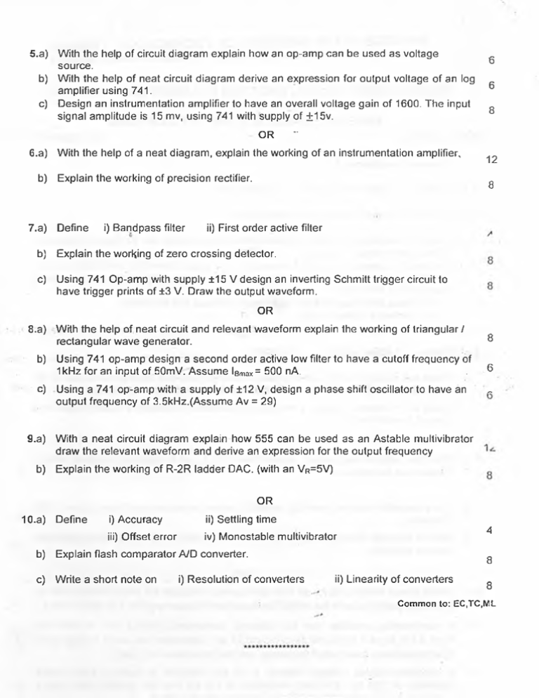
5.a) b) c) With the help of circuit diagram explain how an op-amp can be used as voltage source. With the help of neat circuit diagram derive an expression for output voltage of an log amplifier using 741. Design an instrumentation amplifier to have an overall voltage gain of 1600. The input signal amplitude is 15 mv, using 741 with supply of ±15v. • OR 6.a) b) 7.a) Explain the working of precision rectifier. i) Bandpass filter 6 8 ” With the help of a neat diagram, explain the working of an instrumentation amplifier, Define 6 12 8 ii) First order active filter b) Explain the worKing of zero crossing detector. c) Using 741 Op-amp with supply ±15 V design an inverting Schmitt trigger circuit to have trigger prints of ±3 V. Draw the output waveform. OR 8.a) With the help of neat circuit and relevant waveform explain the working of triangular / rectangular wave generator. b) c) 9.a) b) Using 741 op-amp design a second order active low filter to have a cutoff frequency of 1kHz for an input of 50mV. Assume lemax = 500 nA. . Using a 741 op-amp with a supply of ±12 V, design a phase shift oscillator to have an output frequency of 3.5kHz.(Assume Av = 29) ® 6 « With a neat circuit diagram explain how 555 can be used as an Astable multivibrator draw the relevant waveform and derive an expression for the output frequency Explain the working of R-2R ladder DAC. (with an VR=5V) OR 10.a) Define i) Accuracy ii) Settling time iii) Offset error iv) Monostable multivibrator b) Explain flash comparator A/D converter. c) Write a short note on i) Resolution of converters 4 0 o ii) Linearity of converters 0 o Common to: EC,TC,ML SRI SIDDHARTHA INSTITUTE OF TECHNOLOGY, TUMKUR. (An Autonomous Institution under Visvesvaraya Technological University, Belgaum.) FOURTH SEMESTER B.E., END TERM EXAMINATIONS - JUNE 2011 09DES46 : LINEAR IC’S AND APPLICATIONS TIME: 3.00 Hrs MAX MARKS: 100 A n s w e r the fo llo w in g : 1.a) Define i) Input offset current ii) Slew rate b) Compare voltage follower and emitter follower. c) Explain a technique by which the basic differential amplifier can be made independent of the supply voyage changes. The directly connected voltage follower has a 1V signal, Rs=47kQ, M=200000, ZI=2M, Zo=75Q and a 20kQ load. Calculate the load voltage i) When the load is directly connected to the source ii) When the voltage follower is between the load and the source. iii) Comment on the results d) 4 4 6 OR 2.a) Define i) Offset nulling ii) CMRR b) When two inputs V1 and V2 are applied to inverting and non-inverting terminals of Opamp. Show that the output will be the difference of two with an amplification factor. c) Using a 741 op-amp, design a non-inverting amplifier to amplify a 100mv signal to a level o f 3v with Rs=0 3-a) b) c) 10 With the help of neat circuit, explain how the Z\n of a capacitor coupled voltage follower can be improved. * c For a capacitor coupled inverting amplifier derive an expression to set upper cutoff frequency. , 5 W hat is the need for frequency compensation in op-amp? Explain different techniques that are adopted. 10 OR 4.a) b) c) Define phase margin and for an high gain op-amp calculate the phase margin with an open loop gain of A v with the help of bode plot and discuss whether it is stable or not. 10 A non-inverting amplifier has the following components: R -^33 kQ, R2=150 kQ, R3= 1.5 kQ, R l=4.7 kQ, C-|=0.39 pF, C2=0.27 pF. Determine the circuit voltage gain, input impedance, lower cutoff frequency, and the impedance of C-i at fj. 5 A capacitor-coupled voltage follower is to be designed to have a lower cutoff frequency of 120 Hz. The load resistance is 8.2 kQ and the op-amp used has a maximum input bias current of 600nA. Design a suitable circuit. 5
