DATASHEET
9FGL699
6-OUTPUT LOW POWER DIFFERENTIAL SYNTHESIZER FOR PCIE GEN2
Description
Features/Benefits
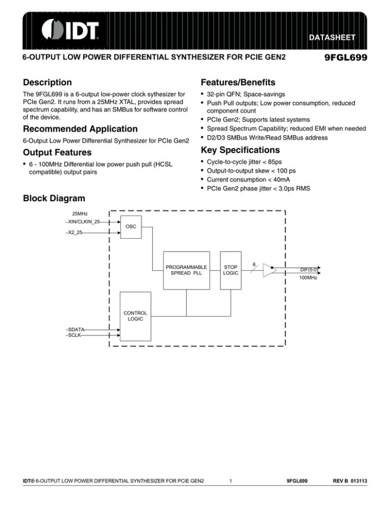
The 9FGL699 is a 6-output low-power clock sythesizer for
PCIe Gen2. It runs from a 25MHz XTAL, provides spread
spectrum capability, and has an SMBus for software control
of the device.
• 32-pin QFN; Space-savings
• Push Pull outputs; Low power consumption, reduced
component count
6-Output Low Power Differential Synthesizer for PCIe Gen2
• PCIe Gen2; Supports latest systems
• Spread Spectrum Capability; reduced EMI when needed
• D2/D3 SMBus Write/Read SMBus address
Output Features
Key Specifications
• 6 - 100MHz Differential low power push pull (HCSL
•
•
•
•
Recommended Application
compatible) output pairs
Cycle-to-cycle jitter < 85ps
Output-to-output skew < 100 ps
Current consumption < 40mA
PCIe Gen2 phase jitter < 3.0ps RMS
Block Diagram
25MHz
XIN/CLKIN_25
OSC
X2_25
PROGRAMMABLE
SPREAD PLL
STOP
LOGIC
6
DIF(5:0)
100MHz
CONTROL
LOGIC
SDATA
SCLK
IDT® 6-OUTPUT LOW POWER DIFFERENTIAL SYNTHESIZER FOR PCIE GEN2
1
9FGL699
REV B 013113
9FGL699
6-OUTPUT LOW POWER DIFFERENTIAL SYNTHESIZER FOR PCIE GEN2
X2 _ 25
X IN /C LK IN _2 5
GN D
NC
V DD
NC
GN D
V DD
Pin Configuration
32 31 30 29 28 27 26 25
NC 1
VDD 2
NC 3
GND 4
24 SMBDAT
23 SMBCLK
22 GND
21 DIF_5
9FGL699
GND 5
DIF_0 6
20 DIF_5#
19 VDD
18 DIF_4
17 DIF_4#
DIF_0# 7
VDD 8
D I F_ 3
D IF _ 3 #
V DD
GN D
D IF _ 2 #
D IF _2
D IF _ 1
D I F_ 1 #
9 10 11 12 13 14 15 16
Power Management
OE (SMBUS)
1
0
Differential Outputs
DIF/DIF# = running
DIF/DIF# = Low/Low
IDT® 6-OUTPUT LOW POWER DIFFERENTIAL SYNTHESIZER FOR PCIE GEN2
2
9FGL699
REV B 013113
9FGL699
6-OUTPUT LOW POWER DIFFERENTIAL SYNTHESIZER FOR PCIE GEN2
Pin Descriptions
Pin#
1
2
3
4
5
6
7
8
9
10
11
12
13
14
15
16
17
18
19
20
21
22
23
24
25
26
27
28
29
30
31
32
Pin Name
NC
Type Pin Description
N/A No Connection.
VDD
NC
GND
GND
DIF_0
DIF_0#
VDD
DIF_1
DIF_1#
DIF_2
DIF_2#
GND
VDD
DIF_3#
DIF_3
DIF_4#
DIF_4
VDD
DIF_5#
DIF_5
GND
SMBCLK
SMBDAT
X2_25
XIN/CLKIN_25
GND
NC
VDD
NC
GND
VDD
PWR
N/A
PWR
PWR
OUT
OUT
PWR
OUT
OUT
OUT
OUT
PWR
PWR
OUT
OUT
OUT
OUT
PWR
OUT
OUT
PWR
IN
I/O
OUT
IN
PWR
N/A
PWR
N/A
PWR
PWR
Power supply, nominal 3.3V
No Connection.
Ground pin.
Ground pin.
0.7V differential true clock output
0.7V differential Complementary clock output
Power supply, nominal 3.3V
0.7V differential true clock output
0.7V differential Complementary clock output
0.7V differential true clock output
0.7V differential Complementary clock output
Ground pin.
Power supply, nominal 3.3V
0.7V differential Complementary clock output
0.7V differential true clock output
0.7V differential Complementary clock output
0.7V differential true clock output
Power supply, nominal 3.3V
0.7V differential Complementary clock output
0.7V differential true clock output
Ground pin.
Clock pin of SMBUS circuitry, 5V tolerant
Data pin of SMBUS circuitry, 5V tolerant
Crystal output, Nominally 25.00MHz.
Crystal input or Reference Clock input. Nominally 25MHz.
Ground pin.
No Connection.
Power supply, nominal 3.3V
No Connection.
Ground pin.
Power supply, nominal 3.3V
IDT® 6-OUTPUT LOW POWER DIFFERENTIAL SYNTHESIZER FOR PCIE GEN2
3
9FGL699
REV B 013113
9FGL699
6-OUTPUT LOW POWER DIFFERENTIAL SYNTHESIZER FOR PCIE GEN2
General SMBus Serial Interface Information for 9FGL699
How to Write
How to Read
•
•
•
•
•
•
•
•
•
•
•
•
•
•
•
•
•
•
•
•
•
Controller (host) sends a start bit
Controller (host) sends the write address
IDT clock will acknowledge
Controller (host) sends the beginning byte location = N
IDT clock will acknowledge
Controller (host) sends the byte count = X
IDT clock will acknowledge
Controller (host) starts sending Byte N through Byte
N+X-1
IDT clock will acknowledge each byte one at a time
Controller (host) sends a Stop bit
Index Block Write Operation
Controller (Host)
T
•
•
•
Index Block Read Operation
IDT (Slave/Receiver)
Controller (Host)
starT bit
T
Slave Address
WR
Controller (host) will send a start bit
Controller (host) sends the write address
IDT clock will acknowledge
Controller (host) sends the beginning byte location = N
IDT clock will acknowledge
Controller (host) will send a separate start bit
Controller (host) sends the read address
IDT clock will acknowledge
IDT clock will send the data byte count = X
IDT clock sends Byte N+X-1
IDT clock sends Byte 0 through Byte X (if X(H) was
written to Byte 8)
Controller (host) will need to acknowledge each byte
Controller (host) will send a not acknowledge bit
Controller (host) will send a stop bit
IDT (Slave/Receiver)
starT bit
Slave Address
WRite
ACK
WR
WRite
ACK
Beginning Byte = N
ACK
Beginning Byte = N
ACK
Data Byte Count = X
ACK
RT
Slave Address
Beginning Byte N
ACK
O
O
RD
ReaD
ACK
X Byte
O
Repeat starT
O
Data Byte Count=X
O
O
ACK
ACK
ACK
Beginning Byte N
Byte N + X - 1
stoP bit
X Byte
P
O
O
O
O
O
O
Read Address
Write Address
D3(H)
D2(H)
IDT® 6-OUTPUT LOW POWER DIFFERENTIAL SYNTHESIZER FOR PCIE GEN2
Byte N + X - 1
N
Not acknowledge
P
stoP bit
4
9FGL699
REV B 013113
9FGL699
6-OUTPUT LOW POWER DIFFERENTIAL SYNTHESIZER FOR PCIE GEN2
SMBus Table: Device Control Register, READ/WRITE ADDRESS (D3/D2)
Byte 0
Pin #
Name
Control Function
Type
Reserved
Bit 7
Reserved
Bit 6
Spread Enable
RW
Bit 5
Reserved
Bit 4
Reserved
Bit 3
Reserved
Bit 2
P
Bit 1
Reserved
Bit 0
0
1
Off
-0.50%
0
1
Disable
Enable
Disable
Enable
Default
0
0
1
0
0
0
0
0
SMBus Table: Output Enable Register
Pin #
Name
Byte 1
Bit 7
DIF_0 EN
Bit 6
Bit 5
Bit 4
DIF_1 EN
Bit 3
Bit 2
Bit 1
Bit 0
Control Function
Type
Reserved
Output Enable
RW
Reserved
Reserved
Output Enable
RW
Reserved
Reserved
Reserved
SMBus Table: Reserved Register
Pin #
Name
Byte 2
Bit 7
Bit 6
Bit 5
Bit 4
Bit 3
Bit 2
Bit 1
Bit 0
Control Function
Type
Reserved
Reserved
Reserved
Reserved
Reserved
Reserved
Reserved
Reserved
0
1
Default
0
0
0
0
0
0
0
0
SMBus Table: Output Enable Register
Pin #
Name
Byte 3
DIF_5 EN
Bit 7
DIF_4 EN
Bit 6
Bit 5
Bit 4
Bit 3
Bit 2
Bit 1
Bit 0
Control Function
Type
Output Enable
RW
Output Enable
RW
Reserved
Reserved
Reserved
Reserved
Reserved
Reserved
0
Disable
Disable
1
Enable
Enable
Default
1
1
0
0
0
0
0
0
IDT® 6-OUTPUT LOW POWER DIFFERENTIAL SYNTHESIZER FOR PCIE GEN2
5
9FGL699
Default
0
1
0
0
1
0
0
0
REV B 013113
9FGL699
6-OUTPUT LOW POWER DIFFERENTIAL SYNTHESIZER FOR PCIE GEN2
SMBus Table:
Byte 4
Bit 7
Bit 6
Bit 5
Bit 4
Bit 3
Bit 2
Bit 1
Bit 0
Reserved Register
Pin #
Name
-
Control Function
Type
Reserved
Reserved
Reserved
Reserved
Reserved
Reserved
Reserved
Reserved
SMBus Table: Output amplitude adjustment
Byte 5
Pin #
Name
Control Function
Bit 7
Type
-
RW
Bit 5
-
RW
DIF_1/2/3 AMP
Bit 3
Bit 2
-
Bit 1
-
Default
0
0
0
0
0
0
0
0
1
Default
0
1
00=700mV
01=800mV
10=900mV
11=1000mV
Amplitude adjustment
RW
0
1
Reserved
Reserved
0
0
00=700mV
01=800mV
10=900mV
11=1000mV
RW
DIF_0 AMP
Bit 0
1
00=700mV
01=800mV
10=900mV
11=1000mV
Amplitude adjustment
Bit 6
-
0
RW
DIF_5/6 AMP
Bit 4
0
Amplitude adjustment
-
RW
SMBus Table:
Byte 6
Bit 7
Bit 6
Bit 5
Bit 4
Bit 3
Bit 2
Bit 1
Bit 0
Reserved Register
Pin #
Name
-
SMBus Table:
Byte 7
Bit 7
Bit 6
Bit 5
Bit 4
Bit 3
Bit 2
Bit 1
Bit 0
Vendor & Revision ID Register
Pin #
Name
Control Function
RID3
RID2
REVISION ID
RID1
RID0
VID3
VID2
VENDOR ID
VID1
VID0
Control Function
Type
Reserved
Reserved
Reserved
Reserved
Reserved
Reserved
Reserved
Reserved
IDT® 6-OUTPUT LOW POWER DIFFERENTIAL SYNTHESIZER FOR PCIE GEN2
Type
R
R
R
R
R
R
R
R
6
0
1
0
1
Default
0
0
0
0
0
0
0
0
0
-
1
-
Default
0
0
0
0
0
0
0
1
9FGL699
REV B 013113
9FGL699
6-OUTPUT LOW POWER DIFFERENTIAL SYNTHESIZER FOR PCIE GEN2
SMBus Table: Reserved Register
Byte 8
Pin #
Name
Bit 7
Bit 6
Bit 5
Bit 4
Bit 3
Bit 2
Bit 1
Bit 0
Control Function
Type
Reserved
Reserved
Reserved
Reserved
Reserved
Reserved
Reserved
Reserved
0
1
Default
0
0
0
0
1
1
1
1
SMBus Table: Output Enable Register
Byte 9
Pin #
Name
Bit 7
Bit 6
DIF_3 EN
Bit 5
DIF_2 EN
Bit 4
Bit 3
Bit 2
Bit 1
Bit 0
Control Function
Type
Reserved
Output Enable
RW
Output Enable
RW
Reserved
Reserved
Reserved
Reserved
Reserved
0
1
Disable
Disable
Enable
Enable
Default
0
1
1
0
0
0
0
0
IDT® 6-OUTPUT LOW POWER DIFFERENTIAL SYNTHESIZER FOR PCIE GEN2
7
9FGL699
REV B 013113
9FGL699
6-OUTPUT LOW POWER DIFFERENTIAL SYNTHESIZER FOR PCIE GEN2
Absolute Maximum Ratings
Stresses above the ratings listed below can cause permanent damage to the 9FGL699. These ratings, which are standard
values for IDT commercially rated parts, are stress ratings only. Functional operation of the device at these or any other
conditions above those indicated in the operational sections of the specifications is not implied. Exposure to absolute
maximum rating conditions for extended periods can affect product reliability. Electrical parameters are guaranteed only over
the recommended operating temperature range.
PARAMETER
SYMBOL
3.3V Logic Supply Voltage
Input Low Voltage
Input High Voltage
Input High Voltage
Storage Temperature
Junction Temperature
Input ESD protection
VDD
VIL
V IH
V IHSMB
Ts
Tj
ESD prot
CONDITIONS
MIN
TYP
MAX
4.6
GND-0.5
Except for SMBus interface
SMBus clock and data pins
VD D+0.5V
5.5V
150
125
-65
Human Body Model
P
UNITS NOTES
V
V
V
V
°
C
°C
V
1,2
1
1
1
1
1
1
1
Guaranteed by design and characterization, not 100% tested in production.
2
Operation under these conditions is neither implied nor guaranteed.
Electrical Characteristics–Input/Supply/Common Output Parameters
TA = TCOM; Supply Voltage VDD = 3.3 V +/-5%
PARAMETER
Ambient Operating
Temperature
Input Frequency
Pin Inductance
SYMBOL
CONDITIONS
MIN
TC OM
Fin
L pin
CIN
CIN XTAL
COUT
Commmercial range
0
X1 pin
Clk Stabilization
TST AB
SS Modulation Frequency
fMODIN
Tfall
Trise
SMBus Input Low Voltage
SMBus Input High Voltage
SMBus Output Low Voltage
SMBus Sink Current
Nominal Bus Voltage
SCLK/SDATA Rise Time
SCLK/SDATA Fall Time
tF
tR
VILSM B
V IHSMB
VOLSMB
I PULLU P
V DD SMB
tR SMB
tFSM B
@ I PULLU P
@ VOL
3V to 5V +/- 10%
(Max VIL - 0.15) to (Min VIH + 0.15)
(Min VIH + 0.15) to (Max VIL - 0.15)
SMBus Operating Frequency
fMAXSMB
Maximum SMBus operating frequency
1
2
MAX
1.5
30
2.1
4
2.7
31.500
UNITS NOTES
1
70
°C
7
5
6
6
MHz
nH
pF
pF
pF
1
1
1
1
1
1.8
ms
1,2
33
kH z
1
5
5
0.8
5.5
1000
300
ns
ns
V
V
V
mA
V
ns
ns
1,2
1,2
1
1
1
1
1
1
1
100
kHz
1
25.000
Logic Inputs
Crystal inputs
Output pin capacitance
From VDD Power-Up and after input clock
stabilization to 1st clock
Allowable Frequency
(Triangular Modulation)
Fall time of control inputs
Rise time of control inputs
Capacitance
TYP
V DD SMB
0.4
Guaranteed by design and characterization, not 100% tested in production.
Control input must be monotonic from 20% to 80% of input swing.
IDT® 6-OUTPUT LOW POWER DIFFERENTIAL SYNTHESIZER FOR PCIE GEN2
8
9FGL699
REV B 013113
9FGL699
6-OUTPUT LOW POWER DIFFERENTIAL SYNTHESIZER FOR PCIE GEN2
Electrical Characteristics–DIF 0.7V Low Power Differential Outputs
TA = TC OM ; Supply Voltage VDD = 3.3 V +/-5%, See Test Loads for loading conditions
PARAMETER
SYMBOL
CONDITIONS
MIN
TYP
MAX
UNITS NOTES
V/ns 1, 2, 3
Scope averaging on
1
4
%
Slew rate matching, Scope averaging on
20
1, 2, 4
Statistical
measurement
on
single-ended
signal
Voltage High
VHigh
660
850
1
using oscilloscope math function. (Scope averaging
mV
Voltage Low
VLow
-150
150
1
on)
Measurement on single ended signal using absolute
Max Voltage
Vmax
1150
1
mV
Min Voltage
Vmin
value. (Scope averaging off)
P
1
Vswing
Vswing
Scope averaging off
300
mV
1, 2
Crossing Voltage (abs)
Vcross_abs
Scope averaging off
300
550
mV
1, 5
Δ-Vcross
Scope averaging off
140
mV
1, 6
Crossing Voltage (var)
1
Guaranteed by design and characterization, not 100% tested in production. CL = 2pF with RS = 33Ω for Zo = 50Ω (100Ω differential trace
impedance).
2
Measured from differential waveform
Slew rate
Slew rate matching
Trf
ΔTrf
3
Slew rate is measured through the Vswing voltage range centered around differential 0V. This results in a +/-150mV window around
differential 0V.
4
Matching applies to rising edge rate of Clock / falling edge rate of Clock#. It is measured in a +/-75mV window centered on the average
cross point where Clock rising meets Clock# falling. The median cross point is used to calculate the voltage thresholds the oscilloscope uses
for the edge rate calculations.
5
Vcross is defined as voltage where Clock = Clock# measured on a component test board and only applies to the differential rising edge (i.e.
Clock rising and Clock# falling).
6
The total variation of all Vcross measurements in any particular system. Note that this is a subset of V_cross_min/max (V_cross absolute)
allowed. The intent is to limit Vcross induced modulation by setting V_cross_delta to be smaller than V_cross abs.
Electrical Characteristics–Current Consumption
TA = TCOM; Supply Voltage VDD = 3.3 V +/-5%, See Test Loads for loading conditions
PARAMETER
SYMBOL
CONDITIONS
Operating Supply Current
1
ID D3. 3
MIN
TYP
VDD, All outputs active @100MHz
MAX
40
UNITS NOTES
mA
1
P
Guaranteed by design and characterization, not 100% tested in production.
Electrical Characteristics–Output Duty Cycle, Jitter, and Skew Characteristics
TA = TCOM; Supply Voltage VDD = 3.3 V +/-5%, See Test Loads for Loading Conditions
PARAMETER
SYMBOL
CONDITIONS
MIN
Duty Cycle
Skew, Output to Output
tDC
t sk3
Measured differentially, PLL Mode
VT = 50%
45
Jitter, Cycle to cycle
tjcyc-cyc
PLL mode
TYP
MAX
UNITS NOTES
55
100
%
ps
1
1
85
ps
1,3
1
Guaranteed by design and characterization, not 100% tested in production.
Measured from differential waveform
3
IDT® 6-OUTPUT LOW POWER DIFFERENTIAL SYNTHESIZER FOR PCIE GEN2
9
9FGL699
REV B 013113
9FGL699
6-OUTPUT LOW POWER DIFFERENTIAL SYNTHESIZER FOR PCIE GEN2
Electrical Characteristics–Phase Jitter Parameters
TA = TCOM; Supply Voltage VDD = 3.3 V +/-5%, See Test Loads for loading conditions
PARAMETER
Phase Jitter, PCI Express
SYMBOL
tjp hPCIeG1
tjp hPCIeG2
CONDITIONS
PCIe Gen 1
PCIe Gen 2 Lo Band
10kHz < f < 1.5MHz
PCIe Gen 2 High Band
1.5MHz < f < Nyquist (50MHz)
MIN
TYP
3
3.1
1
Guaranteed by design and characterization, not 100% tested in production.
2
See http://www.pcisig.com for complete specs
Sample size of at least 100K cycles. This figures extrapolates to 108ps pk-pk @ 1M cycles for a BER of 1-12.
3
6
MAX
86
UNITS Notes
ps (p-p) 1,2,3,6
ps
1,2,6
(rms)
ps
1,2,6
(rms)
Applies to all differential outputs
Low-Power Differential Output Test Load
Zo=100ohm differential
33
2pF
33
2pF
9FGLxxx HCSLcompatible Output
IDT® 6-OUTPUT LOW POWER DIFFERENTIAL SYNTHESIZER FOR PCIE GEN2
10
9FGL699
REV B 013113
9FGL699
6-OUTPUT LOW POWER DIFFERENTIAL SYNTHESIZER FOR PCIE GEN2
Thermal Characteristics
Parameter
Symbol
Thermal Resistance Junction to
Ambient
Thermal Resistance Junction to Case
Conditions
Min.
Typ.
Max. Units
JA
Still air
34
C/W
JA
1 m/s air flow
29
C/W
JA
3 m/s air flow
27
C/W
32
C/W
JC
Marking Diagram
ICS
FGL699AL
YYWW
COO
LOT
Notes:
1. ‘LOT’ is the lot number.
2. ‘COO’ is country of origin.
3. YYWW is the last two digits of the year and week that the part was assembled.
4. “L” denotes RoHS compliant package.
IDT® 6-OUTPUT LOW POWER DIFFERENTIAL SYNTHESIZER FOR PCIE GEN2
11
9FGL699
REV B 013113
9FGL699
6-OUTPUT LOW POWER DIFFERENTIAL SYNTHESIZER FOR PCIE GEN2
Package Outline and Package Dimensions (32-pin MLF)
Seating Plane
A1
Index Area
N
1
2
(Ref)
ND & NE
Even
(ND-1)x e
(Ref)
L
A3
e
N
Anvil
Singulation
1
(Typ)
If ND & NE
2
are Even
2
E
-- or -Top View
E2
E2
Sawn
Singulation
A
D
0.08 C
(NE-1)x e
(Ref)
2
(Ref)
ND & NE
Odd
b
e
C
Symbol
Millimeters
Min
Max
A
A1
A3
b
e
D x E BASIC
D2 MIN./MAX.
E2 MIN./MAX.
L MIN./MAX.
N
ND
NE
0.8
1.0
0
0.05
0.20 Reference
0.18
0.3
0.50 BASIC
5.00 x 5.00
3.00
3.30
3.00
3.30
0.30
0.50
32
8
8
Thermal Base
D2
2
D2
Ordering Information
Part / Order Number
Marking
Shipping Packaging
Package
Temperature
9FGL699AKLF
9FGL699AKLFT
see page 11
Trays
Tape and Reel
32-pin MLF
32-pin MLF
0 to +70 C
0 to +70 C
"LF" suffix to the part number are the Pb-Free configuration, RoHS compliant.
“A” is the device revision designator (will not correlate with the datasheet revision).
While the information presented herein has been checked for both accuracy and reliability, Integrated Device Technology (IDT) assumes
no responsibility for either its use or for the infringement of any patents or other rights of third parties, which would result from its use. No
other circuits, patents, or licenses are implied. This product is intended for use in normal commercial applications. Any other applications
such as those requiring extended temperature range, high reliability, or other extraordinary environmental requirements are not
recommended without additional processing by IDT. IDT reserves the right to change any circuitry or specifications without notice. IDT
does not authorize or warrant any IDT product for use in life support devices or critical medical instruments.
IDT® 6-OUTPUT LOW POWER DIFFERENTIAL SYNTHESIZER FOR PCIE GEN2
12
9FGL699
REV B 013113
9FGL699
6-OUTPUT LOW POWER DIFFERENTIAL SYNTHESIZER FOR PCIE GEN2
Revision History
Rev.
A
B
Issue Date WHO Description
04/05/12
AT Released to Final
Updated Cycle-to-cycle jitter max spec from 125ps to 85ps
01/31/13
AT
per latest characterization data.
IDT® 6-OUTPUT LOW POWER DIFFERENTIAL SYNTHESIZER FOR PCIE GEN2
13
Page #
9
9FGL699
REV B 013113
9FGL699
6-OUTPUT LOW POWER DIFFERENTIAL SYNTHESIZER FOR PCIE GEN2
SYNTHESIZERS
Innovate with IDT and accelerate your future networks. Contact:
www.IDT.com
For Sales
For Tech Support
800-345-7015
408-284-8200
Fax: 408-284-2775
www.idt.com/go/clockhelp
pcclockhelp@idt.com
Corporate Headquarters
Integrated Device Technology, Inc.
www.idt.com
© 2010 Integrated Device Technology, Inc. All rights reserved. Product specifications subject to change without notice. IDT, ICS, and the IDT logo are trademarks of Integrated
Device Technology, Inc. Accelerated Thinking is a service mark of Integrated Device Technology, Inc. All other brands, product names and marks are or may be trademarks or
registered trademarks used to identify products or services of their respective owners.
Printed in USA


