DATASHEET
LOW PHASE NOISE ZERO DELAY BUFFER AND MULTIPLIER
Description
Features
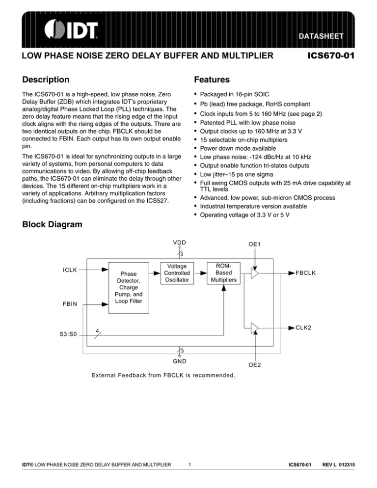
The ICS670-01 is a high-speed, low phase noise, Zero
Delay Buffer (ZDB) which integrates IDT’s proprietary
analog/digital Phase Locked Loop (PLL) techniques. The
zero delay feature means that the rising edge of the input
clock aligns with the rising edges of the outputs. There are
two identical outputs on the chip. FBCLK should be
connected to FBIN. Each output has its own output enable
pin.
•
•
•
•
•
•
•
•
•
•
•
The ICS670-01 is ideal for synchronizing outputs in a large
variety of systems, from personal computers to data
communications to video. By allowing off-chip feedback
paths, the ICS670-01 can eliminate the delay through other
devices. The 15 different on-chip multipliers work in a
variety of applications. Arbitrary multiplication factors
(including fractions) can be configured on the ICS527.
•
•
•
ICS670-01
Packaged in 16-pin SOIC
Pb (lead) free package, RoHS compliant
Clock inputs from 5 to 160 MHz (see page 2)
Patented PLL with low phase noise
Output clocks up to 160 MHz at 3.3 V
15 selectable on-chip multipliers
Power down mode available
Low phase noise: -124 dBc/Hz at 10 kHz
Output enable function tri-states outputs
Low jitter–15 ps one sigma
Full swing CMOS outputs with 25 mA drive capability at
TTL levels
Advanced, low power, sub-micron CMOS process
Industrial temperature version available
Operating voltage of 3.3 V or 5 V
Block Diagram
VDD
OE1
3
ICLK
Phase
Detector,
Charge
Pump, and
Loop Filter
FBIN
S3:S0
Voltage
Controlled
Oscillator
ROMBased
Multipliers
FBCLK
CLK2
4
3
GND
OE2
External Feedback from FBCLK is recommended.
IDT® LOW PHASE NOISE ZERO DELAY BUFFER AND MULTIPLIER
1
ICS670-01
REV L 012315
ICS670-01
LOW PHASE NOISE ZERO DELAY BUFFER AND MULTIPLIER
Pin Assignment
ZDB AND MULTIPLIER
Multiplier Select Table
S3
S2
S1
S0
CLK2 (and FBCLK)
Input Range (MHz)
0
0
0
0
Low (Power down entire
chip)
-
GND
0
0
0
1
Input x1.333
18 - 120
0
1
0
Input x6
5 - 26.67
VDD
1
16
GND
VDD
2
15
GND
VDD
3
14
CLK2
4
13
S0
0
OE2
5
12
S1
0
0
1
1
Input x1.5
16.67 - 107
1
0
0
Input x3.333
7.5 - 48
FBCLK
6
11
S2
0
OE1
7
10
S3
0
1
0
1
Input x2.50
10 - 64
ICLK
0
1
1
0
Input x4
6 - 40
0
1
1
1
Input x1
25 - 160
1
0
0
0
Input x2.333
11 - 69
1
0
0
1
Input x2.666
10 - 60
1
0
1
0
Input x12
5 - 13.33
1
0
1
1
Input x3
8 - 53.33
1
1
0
0
Input x10
5 - 16
1
1
0
1
Input x5
6 - 32
1
1
1
0
Input x8
5 - 20
1
1
1
1
Input x2
12 - 80
9
8
FBIN
Pin Descriptions
Pin
Number
Pin
Name
Pin
Type
Pin Description
1-3
VDD
Input
Power supply. Connect all pins to the same voltage (either 3.3 V or 5 V). Pins
1 and 2 supply the analog sections of the chip.
4
CLK2
5
OE2
6
FBCLK
7
OE1
Input
Output clock enable 1. Tri-states the feedback clock output when low.
8
FBIN
Input
Feedback clock input.
9
ICLK
Input
Clock input. Connect to a 5 - 210 MHz clock.
10
S3
Input
Multiplier select pin 3. Determines outputs per table above. Internal pull-up.
11
S2
Input
Multiplier select pin 2. Determines outputs per table above. Internal pull-up.
12
S1
Input
Multiplier select pin 1. Determines outputs per table above. Internal pull-up.
13
S0
Input
Multiplier select pin 0. Determines outputs per table above. Internal pull-up.
14 - 16
GND
Power
Connect to ground.
Output Clock output from VCO. Output frequency equals the input frequency times
multiplier.
Input
Output clock enable 2. Tri-states the clock 2 output when low.
Output Clock output from VCO. Output frequency equals the input frequency times
multiplier.
IDT® LOW PHASE NOISE ZERO DELAY BUFFER AND MULTIPLIER
2
ICS670-01
REV L 012315
ICS670-01
LOW PHASE NOISE ZERO DELAY BUFFER AND MULTIPLIER
ZDB AND MULTIPLIER
External Components
The ICS670-01 requires a minimum number of external components for proper operation. Decoupling capacitors of
0.01µF should be connected from each VDD pin to the ground plane, as close to the device as possible. A series
termination resistor of 33 should be used to each clock output pin.
Absolute Maximum Ratings
Stresses above the ratings listed below can cause permanent damage to the ICS670-01. These ratings, which are
standard values for IDT commercially rated parts, are stress ratings only. Functional operation of the device at these
or any other conditions above those indicated in the operational sections of the specifications is not implied.
Exposure to absolute maximum rating conditions for extended periods can affect product reliability. Electrical
parameters are guaranteed only over the recommended operating temperature range.
Item
Rating
Supply Voltage, VDD
7V
All Inputs and Outputs
-0.5 V to VDD+0.5 V
Ambient Operating Temperature
0 to +70C
Ambient Operating Temperature, ICS670-01I
-40 to +85C
Storage Temperature
-65 to +150C
Junction Temperature
125C
Soldering Temperature
260C
Recommended Operation Conditions
Parameter
Min.
Ambient Operating Temperature
Power Supply Voltage (measured in respect to GND)
Typ.
Max.
Units
0
+70
C
+3.0
+5.5
V
DC Electrical Characteristics
VDD=3.3V ±10%, Ambient temperature -40 to +85C, unless stated otherwise
Parameter
Symbol
Conditions
Min.
Typ.
Max.
Units
5.5
V
Operating Voltage
VDD
3.0
Input High Voltage
VIH
2
Input Low Voltage
VIL
Output High Voltage
VOH
IOH = -12 mA
Output Low Voltage
VOL
IOL = 12 mA
Output High Voltage,
CMOS level
VOH
IOH = -4 mA
Operating Supply Current
IDD
No Load
35
mA
Short Circuit Current
IOS
Each output
±50
mA
Internal Pull-up Resistor
RPU
OE, select pins
200
k
Input Capacitance
CIN
OE, select pins
5
pF
V
0.8
IDT® LOW PHASE NOISE ZERO DELAY BUFFER AND MULTIPLIER
3
2.4
V
V
0.4
VDD-0.4
V
V
ICS670-01
REV L 012315
ICS670-01
LOW PHASE NOISE ZERO DELAY BUFFER AND MULTIPLIER
ZDB AND MULTIPLIER
AC Electrical Characteristics
VDD = 3.3V ±10%, Ambient Temperature -40 to +85C, unless stated otherwise
Parameter
Input Clock Frequency
Symbol
fIN
Conditions
Min.
See table on page 2
Typ.
5
Output Clock Frequency
PLL Stabilization Time
tSTAB
Input frequency 5 MHz to 160 MHz
4
Max. Units
160
MHz
160
MHz
10
µs
Output Rise Time
tOR
0.8 to 2.0 V, no load
1.5
ns
Output Fall Time
tOF
2.0 to 0.8 V, no load
1.5
ns
Output Clock Duty Cycle
tDC
measured at VDD/2
55
%
45
50
Input to Output Skew
Note 1
±100
ps
Maximum Absolute Jitter
short term
±45
ps
Maximum Jitter
one sigma
15
ps
Phase Noise, relative to
carrier, 125 MHz (x5)
100 Hz offset
-110
dBc/Hz
1 kHz offset
-122
dBc/Hz
10 kHz
-124
dBc/Hz
200 kHz
-117
dBc/Hz
Note 1: Rising edge of ICLK compared with rising edge of CLK2, with FBCLK connected to FBIN, and
15 pF load on CLK2. See graph on page 5 for skew vs. frequency and loading.
Thermal Characteristics
Parameter
Thermal Resistance Junction to
Ambient
Thermal Resistance Junction to Case
Symbol
Conditions
Min.
Typ.
Max. Units
JA
Still air
120
C/W
JA
1 m/s air flow
115
C/W
JA
3 m/s air flow
105
C/W
58
C/W
JC
IDT® LOW PHASE NOISE ZERO DELAY BUFFER AND MULTIPLIER
4
ICS670-01
REV L 012315
ICS670-01
LOW PHASE NOISE ZERO DELAY BUFFER AND MULTIPLIER
ZDB AND MULTIPLIER
Figure 1. Skew from ICLK to CLK2, with change in load capacitance (VDD = 3.3V)
300
200
Skew (ps)
100
0
-100
25
50
75
100
125
150
-200
-300
-400
CLK2 Frequency (MHz)
Skew (ps) 20 pF
Skew (ps) 10 pF
Adjusting Input/Output Skew
The data in Figure 1 can be used to adjust individual circuit characteristics and achieve the minimum possible skew
between ICLK and CLK2. With a 125 MHz output, for example, having a total load capacitance of 15 pF will result
in nearly zero skew between ICLK and CLK2. Note that the load
capacitance includes board trace capacitance, input capacitance of the load being driven by the ICS670-01, and
any additional capacitors connected to CLK2.
Figure 2. Phase Noise for 125 MHz output, 25 MHz clock input (VDD = 3.3V)
ICS670 Phase noise
0
-20
-40
L(f) dBc
-60
-80
-100
-120
-140
10.E+0
100.E+0
1.E+3
10.E+3
100.E+3
1.E+6
10.E+6
offset frequency
IDT® LOW PHASE NOISE ZERO DELAY BUFFER AND MULTIPLIER
5
ICS670-01
REV L 012315
ICS670-01
LOW PHASE NOISE ZERO DELAY BUFFER AND MULTIPLIER
ZDB AND MULTIPLIER
Package Outline and Package Dimensions (16-pin SOIC, 150 Mil. Narrow Body)
Package dimensions are kept current with JEDEC Publication No. 95
16
Millimeters
Symbol
E
Min
A
A1
B
C
D
E
e
H
h
L
H
INDEX
AREA
1 2
D
A
Inches
Max
Min
1.35
1.75
0.10
0.25
0.33
0.51
0.19
0.25
9.80
10.00
3.80
4.00
1.27 BASIC
5.80
6.20
0.25
0.50
0.40
1.27
0
8
Max
.0532
.0688
.0040
.0098
.013
.020
.0075
.0098
.3859
.3937
.1497
.1574
0.050 BASIC
.2284
.2440
.010
.020
.016
.050
0
8
h x 45
A1
C
-Ce
SEATING
PLANE
B
L
.10 (.004)
C
Ordering Information
Part / Order Number
Marking
Shipping Packaging
Package
Temperature
670M-01LF
670M-01LFT
670M-01ILF
670M-01ILFT
670M-01LF
670M-01LF
670M-01ILF
670M-01ILF
Tubes
Tape and Reel
Tubes
Tape and Reel
16-pin SOIC
16-pin SOIC
16-pin SOIC
16-pin SOIC
0 to +70 C
0 to +70 C
-40 to +85 C
-40 to +85 C
"LF" suffix to the part number denotes Pb-Free configuration, RoHS compliant.
While the information presented herein has been checked for both accuracy and reliability, Integrated Device Technology (IDT) assumes no responsibility
for either its use or for the infringement of any patents or other rights of third parties, which would result from its use. No other circuits, patents, or licenses
are implied. This product is intended for use in normal commercial applications. Any other applications such as those requiring extended temperature range,
high reliability, or other extraordinary environmental requirements are not recommended without additional processing by IDT. IDT reserves the right to
change any circuitry or specifications without notice. IDT does not authorize or warrant any IDT product for use in life support devices or critical medical
instruments.
Revision History
Rev.
Date
Originator
L
01/23/15
RDW
Description of Change
Updated AC characterization table with new parameter "PLL Stabilization Time".
IDT® LOW PHASE NOISE ZERO DELAY BUFFER AND MULTIPLIER
6
ICS670-01
REV L 012315
ICS670-01
LOW PHASE NOISE ZERO DELAY BUFFER AND MULTIPLIER
ZDB AND MULTIPLIER
Innovate with IDT and accelerate your future networks. Contact:
www.IDT.com
For Sales
For Tech Support
800-345-7015
408-284-8200
Fax: 408-284-2775
www.idt.com/go/clockhelp
Corporate Headquarters
Integrated Device Technology, Inc.
www.idt.com
© 2015 Integrated Device Technology, Inc. All rights reserved. Product specifications subject to change without notice. IDT and the IDT logo are trademarks of Integrated Device
Technology, Inc. Accelerated Thinking is a service mark of Integrated Device Technology, Inc. All other brands, product names and marks are or may be trademarks or registered
trademarks used to identify products or services of their respective owners.
Printed in USA


