MPQ2249
Industrial Grade
6V, 3A, 1MHz, Low-Voltage
Synchronous Step-Down Converter
The Future of Analog IC Technology
DESCRIPTION
FEATURES
•
•
•
•
•
•
•
•
•
•
The MPQ2249 is a 1MHz constant frequency,
current mode, PWM step-down converter. The
device integrates a main switch and a
synchronous rectifier for high efficiency and
eliminates the need for an external Schottky
diode. It is ideal for powering portable
equipment that runs from a single cell LithiumIon (Li+) battery.
The MPQ2249 can supply 3A of load current
from a 2.5V to 6V input voltage. It can run at
100% duty cycle for low dropout applications.
The MPQ2249 provides internal soft-start
control to reduce rush current and output
discharge function to control discharging of the
output capacitor.
•
•
•
High Efficiency: Up to 90%
Power Save Mode at Light Load
1MHz Constant Switching Frequency
Up to 4.5A PeakCurrent
2.5V to 6V Input Voltage Range
Output Adjustable from 0.6V to VIN
100% Duty Cycle in Dropout
Output Discharge Function
Internal Soft-Start Control
Power Good Indicator
Short Circuit Protection
Thermal Fault Protection
Available in SOIC8E Package
APPLICATIONS
•
•
•
•
•
•
The MPQ2249 is available in small SOIC8E
package.
Cellular and Smart Phones
Microprocessors and DSP Core Supplies
PDAs
MP3 Players
Digital Still and Video Cameras
Portable Instruments
All MPS parts are lead-free and adhere to the RoHS directive. For MPS green
status, please visit MPS website under Quality Assurance. “MPS” and “The
Future of Analog IC Technology” are Registered Trademarks of Monolithic
Power Systems, Inc.
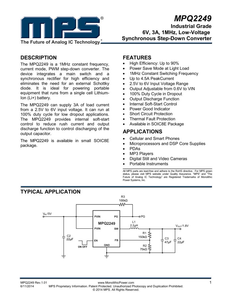
TYPICAL APPLICATION
R3
VIN / 5V
PVIN
PG
PG
MPQ2249
PVIN
L1
2.2 H
VOUT /1.8V
SW
R1
C2
ON OFF
C3
FB
EN
GND
C4
R2
MPQ2249 Rev.1.01
www.MonolithicPower.com
6/11/2014
MPS Proprietary Information. Patent Protected. Unauthorized Photocopy and Duplication Prohibited.
© 2014 MPS. All Rights Reserved.
1
MPQ2249 – INDUSTRIAL GRADE, 6V, 3A, 1MHZ, LOW-VOLTAGE SYNCHRONOUS STEP-DOWN CONVERTER
ORDERING INFORMATION
Part Number
Package
Top Marking
MPQ2249DN
SOIC8E
MP2249
For Tape and Reel, add suffix -Z (e.g. MPQ2249DN–Z).
For RoHS Compliant Packaging, add suffix - LF (e.g. MPQ2249DN–LF–Z);
PACKAGE REFERENCE
SOIC8E
ABSOLUTE MAXIMUM RATINGS (1)
Thermal Resistance
PVIN to GND .............................. -0.3V to +6.5V
SW to GND ............................-0.3V to VIN +0.3V
FB, EN & PG to GND .................. -0.3V to +6.5V
Junction Temperature ............................ +150°C
Continuous Power Dissipation (TA = +25°C) (2)
SOIC8E .....................................................2.5W
Lead Temperature ................................. +260°C
Storage Temperature .............. -65°C to +150°C
SOIC8E .................................. 50 ...... 10 ... °C/W
Recommended Operating Conditions
(3)
Supply Voltage VIN ............................ 2.5V to 6V
Output Voltage VOUT.......................... 0.6V to 6V
Operating Junct. Temp. ........... -40°C to +125°C
(4)
θJA
θJC
Notes:
1) Exceeding these ratings may damage the device.
2) The maximum allowable power dissipation is a function of the
maximum junction temperature. TJ(MAX) the junction-toambient thermal resistance θJA and the ambient temperature
TA. The maximum allowable power dissipation at any ambient
temperature is calculated using: PD(MAX)=(TJ(MAX)-TA)/ θJA.
Exceeding the maximum allowable power dissipation will
cause excessive die temperature, and the regulator will go
into thermal shutdown. Internal thermal shutdown circuitry
protects the device from permanent damage.
3) The device is not guaranteed to function outside of its
operating conditions.
4) Measured on JESD51-7, 4-layer PCB.
MPQ2249 Rev.1.01
www.MonolithicPower.com
6/11/2014
MPS Proprietary Information. Patent Protected. Unauthorized Photocopy and Duplication Prohibited.
© 2014 MPS. All Rights Reserved.
2
MPQ2249 – INDUSTRIAL GRADE, 6V, 3A, 1MHZ, LOW-VOLTAGE SYNCHRONOUS STEP-DOWN CONVERTER
ELECTRICAL CHARACTERISTICS
VIN = VEN = 3.6V, TJ = -40°C to +125°C, typical values are at TJ=+25°C, unless otherwise noted.
Parameter
Symbol Condition
Supply Current
IQ
Shutdown Current
IN Under Voltage Lockout
(UVLO) Threshold
IN Under Voltage Lockout
Hysteresis
Soft-Start Time
Discharge
MOSFET
On
Resistance
Regulated FB Voltage
FB Input Bias Current
PFET On Resistance
NFET On Resistance
SW Leakage Current
(5)
PFET Current Limit
VEN = VIN, VFB = 0.51V
VEN = 0V, TJ = 25°C
VEN = 0V
Rising Edge
VFB
ILIMIT
Min
2.15
Typ
Max
Units
600
0.01
0.01
750
1
10
μA
μA
μA
2.3
2.45
V
210
mV
1
ms
100
Ω
TA = +25°C
0.594
0.600
0.606
-40°C ≤ TA ≤ +125°C
VFB = 0.65V
0.588
-50
0.600
0.5
0.612
+50
ISW = 100mA
ISW = -100mA
VEN = 0V,VIN = 6V,
VSW = 0V or 6V
Duty Cycle = 100%,
Current Pulse Width
< 1ms
92
72
-1
V
nA
mΩ
mΩ
+1
μA
4.5
A
Oscillator Frequency
fSW
1
MHz
(5)
tON
100
ns
145
°C
Minimum On Time
Thermal
Shutdown
(5)
Threshold
Trip
EN Turn-on Trip Threshold
-40°C ≤ TA ≤ +125°C
EN Turn-off Trip Threshold
-40°C ≤ TA ≤ +125°C
25°C
-40°C = TA = +125°C
EN-pull down resistor
Latch Off Under Voltage (UV)
(5)
Threshold
PG Upper Trip Threshold
PG Lower Trip Threshold
PG Output Low Voltage
ISINK=1mA
1.8
0.4
340
300
V
V
400
540
620
kΩ
67%
VFB
90%
85%
VFB
VFB
V
0.3
Notes:
5) Guarantee by design, no production test.
MPQ2249 Rev.1.01
www.MonolithicPower.com
6/11/2014
MPS Proprietary Information. Patent Protected. Unauthorized Photocopy and Duplication Prohibited.
© 2014 MPS. All Rights Reserved.
3
MPQ2249 – INDUSTRIAL GRADE, 6V, 3A, 1MHZ, LOW-VOLTAGE SYNCHRONOUS STEP-DOWN CONVERTER
TYPICAL PERFORMANCE CHARACTERISTICS
VIN = 5V, EN = 5V, VO = 1.8V, L1 = 2.2µH, and TA = +25°C, unless otherwise noted.
100
Load Efficiency
Line Efficiency
VOUT=1.8V
VOUT=1.8V
100
Line Regulation
VOUT=1.8V
1.90
VIN=3V
80
80
VIN=4V
70
IOUT=2A
IOUT=1A
1.78
IOUT=2A
60
VIN=6V
50
0.0
0.5 1.0 1.5 2.0 2.5
LOAD CURRENT ( A )
3.0
1.74
50
2.5
3.1 3.7 4.3 4.9 5.5
LOAD CURRENT ( A )
Load Regulation
Load Efficiency
VOUT=1.8V
VOUT=3.3V
100
1.70
2.5
6.1
VIN=5V
1.77
1.75
0.0
0.5 1.0 1.5 2.0 2.5
LOAD CURRENT ( A )
VIN=5V
80
VIN=6V
50
0.0
75
0.5 1.0 1.5 2.0 2.5
LOAD CURRENT ( A )
Line Regulation
Load Regulation
VOUT=3.3V
VOUT=3.3V
3.40
3.36
3.28
3.28
3.24
3.20
4.5
VIN=5.5V
3.24
4.8
5.1
5.4
5.7
LOAD CURRENT ( A )
6.0
3.20
0.0
6.0
5.5
3.32
IOUT=2A
4.8
5.1
5.4
5.7
LOAD CURRENT ( A )
Peak Current vs.
Duty Cycle
VIN=4.5V
3.32
70
4.5
3.0
3.36
IOUT=1A
IOUT=2A
85
VIN=5.5V
60
3.0
90
VIN=4.5V
70
1.79
IOUT=1A
95
80
VIN=3V
6.1
VOUT=3.3V
100
PEAK CURRENT ( A )
1.81
3.1 3.7 4.3 4.9 5.5
LOAD CURRENT ( A )
Line Efficiency
90
1.83
3.40
1.82
IOUT=1A
70
VIN=5V
60
1.85
1.86
90
90
0.5 1.0 1.5 2.0 2.5
LOAD CURRENT ( A )
3.0
5.2
4.9
4.6
4.3
4.0
20
30
40
50
MPQ2249 Rev.1.01
www.MonolithicPower.com
6/11/2014
MPS Proprietary Information. Patent Protected. Unauthorized Photocopy and Duplication Prohibited.
© 2014 MPS. All Rights Reserved.
60
70
80
90
4
MPQ2249 – INDUSTRIAL GRADE, 6V, 3A, 1MHZ, LOW-VOLTAGE SYNCHRONOUS STEP-DOWN CONVERTER
TYPICAL PERFORMANCE CHARACTERISTICS (continued)
VIN = 5V, EN = 5V, VO = 1.8V, L1 = 2.2µH, and TA = +25°C, unless otherwise noted.
VOUT Voltage vs. TA
IQ Current vs. TA
620
2.0
600
610
1.9
560
1.8
520
1.7
480
1.6
440
VOUT VOLTAGE ( V )
VFB VOLTAGE ( mV )
VFB Voltage vs. TA
600
590
580
570
-40
-10
20
50
80 110 140
1.5
-40
-10
20
50
80 110 140
400
-40
-10
20
50
80 110 140
FSW Frequency vs. TA
FSW FREQUENCY ( MHz )
1.5
1.3
1.1
0.9
0.7
0.5
-40
-10
20
50
80 110 140
MPQ2249 Rev.1.01
www.MonolithicPower.com
6/11/2014
MPS Proprietary Information. Patent Protected. Unauthorized Photocopy and Duplication Prohibited.
© 2014 MPS. All Rights Reserved.
5
MPQ2249 – INDUSTRIAL GRADE, 6V, 3A, 1MHZ, LOW-VOLTAGE SYNCHRONOUS STEP-DOWN CONVERTER
TYPICAL PERFORMANCE CHARACTERISTICS (continued)
VIN = 5V, EN = 5V, VO = 1.8V, L1 = 2.2µH, and TA = +25°C, unless otherwise noted.
Steady State Operation
Steady State Operation
Start-up through EN
IOUT=0A
IOUT=3A
IOUT=0A
VOUT/AC
50mV/div
VOUT/AC
50mV/div
VOUT
1V/div
SW
2V/div
SW
2V/div
IL
500mA/div
IL
5A/div
PG
5V/div
EN
5V/div
Shut-down through EN
Start-up through EN
Shut-down through EN
IOUT=0A
IOUT=3A
IOUT=3A
VOUT
1V/div
VOUT
1V/div
VOUT
1V/div
PG
5V/div
PG
5V/div
PG
5V/div
EN
5V/div
EN
5V/div
EN
5V/div
Short Circuit Protection
Short Circuit Protection
Load Transient
IOUT=0A to short
IOUT=3A to short
IOUT=1.5A to 3A
VOUT
1V/div
VOUT
1V/div
SW
2V/div
SW
2V/div
IL
5A/div
IL
5A/div
VOUT/AC
50mV/div
SW
5V/div
IL
2A/div
MPQ2249 Rev.1.01
www.MonolithicPower.com
6/11/2014
MPS Proprietary Information. Patent Protected. Unauthorized Photocopy and Duplication Prohibited.
© 2014 MPS. All Rights Reserved.
6
MPQ2249 – INDUSTRIAL GRADE, 6V, 3A, 1MHZ, LOW-VOLTAGE SYNCHRONOUS STEP-DOWN CONVERTER
TYPICAL PERFORMANCE CHARACTERISTICS (continued)
VIN = 5V, EN = 5V, VO = 1.8V, L1 = 2.2µH, and TA = +25°C, unless otherwise noted.
Power Ramp Up
Power Ramp Down
VIN=2.5V, IOUT=3A
VIN=2.5V, IOUT=3A
VIN
2V/div.
VIN
2V/div.
VSW
2V/div.
VSW
2V/div.
VOUT
2V/div.
VOUT
2V/div.
IL
2A/div.
IL
2A/div.
MPQ2249 Rev.1.01
www.MonolithicPower.com
6/11/2014
MPS Proprietary Information. Patent Protected. Unauthorized Photocopy and Duplication Prohibited.
© 2014 MPS. All Rights Reserved.
7
MPQ2249 – INDUSTRIAL GRADE, 6V, 3A, 1MHZ, LOW-VOLTAGE SYNCHRONOUS STEP-DOWN CONVERTER
PIN FUNCTIONS
Pin #
SOIC8E
Name
5, 6
SW
Power Switch Output. Inductor connection to drains of the internal PFET and NFET
switches.
7
PG
Power-good indicator. PG is pulled low when output is outside the window of regulation
or the device enters shutdown.
8
EN
Regulator Enable Control Input. Drive EN above 1.8V to turn on the MPQ2249. Drive EN
below 0.4V to turn it off. EN is pulled to GND with a 450kΩ internal resistor.
1
FB
Feedback Input. Connect FB to the center point of the external resistor divider. The
feedback threshold voltage is 0.6V.
2, 3
Exposed
Pad
4
Description
GND
Ground. Connect Exposed Pad to ground plane for optimal thermal performance.
PVIN
Power Stage Supply Input. Bypass to GND with a 2.2μF or bigger ceramic capacitor.
MPQ2249 Rev.1.01
www.MonolithicPower.com
6/11/2014
MPS Proprietary Information. Patent Protected. Unauthorized Photocopy and Duplication Prohibited.
© 2014 MPS. All Rights Reserved.
8
MPQ2249 – INDUSTRIAL GRADE, 6V, 3A, 1MHZ, LOW-VOLTAGE SYNCHRONOUS STEP-DOWN CONVERTER
FUNCTION BLOCK DIAGRAM
PVIN
EN
PVIN
BIAS &
VOLTAGE
REFERENCE
0.6V
0.4V
1MHz
OSCILLATOR
MAIN
SWITCH
PCH
ISLOPE
OSC
Internal SS
FB
CONTROL
LOGIC
COMP
0.6V
PWM
600k
SW
34pF
1pF
0.4V
PG
SYNCHRONOUS
RECTIFIER
NCH
OUTPUT
DISCHARGE
R
0.54V
LOW SIDE
GATE DRIVE
GND
Figure 1—Function Block Diagram
OPERATION
The MPQ2249 is a constant frequency current
mode PWM step-down converter. The MPQ2249
is optimized for low voltage, Li-Ion battery
powered applications where high efficiency and
small size are critical. The MPQ2249 uses an
external resistor divider to set the output voltage
from 0.6V to 6V. The device integrates both a
main switch and synchronous rectifier, which
provides high efficiency and eliminates an
external Schottky diode. The MPQ2249 can
achieve 100% duty cycle. The duty cycle D of a
step-down converter is defined as:
D = TON × f OSC × 100% ≈
VOUT
× 100%
VIN
Where TON is the main switch on time, fOSC is the
oscillator frequency (1MHz), VOUT is the output
voltage and VIN is the input voltage
Current Mode PWM Control
Slope compensated current mode PWM control
provides stable switching and cycle-by-cycle
current limit for superior load and line response
and protection of the internal main switch and
synchronous rectifier. The MPQ2249 switches at
a constant frequency (1MHz) and regulates the
output voltage. During each cycle the PWM
comparator modulates the power transferred to
the load by changing the inductor peak current
based on the feedback error voltage. During
normal operation, the main switch is turned on for
a certain time to ramp the inductor current at
each rising edge of the internal oscillator, and
switched off when the peak inductor current is
above the error voltage. When the main switch is
off, the synchronous rectifier will be turned on
immediately.
MPQ2249 Rev.1.01
www.MonolithicPower.com
6/11/2014
MPS Proprietary Information. Patent Protected. Unauthorized Photocopy and Duplication Prohibited.
© 2014 MPS. All Rights Reserved.
9
MPQ2249 – INDUSTRIAL GRADE, 6V, 3A, 1MHZ, LOW-VOLTAGE SYNCHRONOUS STEP-DOWN CONVERTER
Power Save Mode Operation
The MPQ2249 enters asynchronous mode as
soon as current of LS MOS goes below zero.
When the load is light enough and comp voltage is
lower than the set value, the part goes into power
skipping mode. This mode improves efficiency at
light load condition.
Dropout Operation
The MPQ2249 allows the main switch to remain on
for more than one switching cycle and increases
the duty cycle while the input voltage is dropping
close to the output voltage. When the duty cycle
reaches 100%, the main switch is held on
continuously to deliver current to the output up to
the switch’s current limit. The output voltage then is
the input voltage minus the voltage drop across the
main switch and the inductor.
Over-Current-Protection and Latchoff
The MPQ2249 provides cycle-by-cycle over current
limit when inductor current peak value exceeds the
current limit threshold. Meanwhile, output voltage
starts to drop until FB is below the Under-Voltage
(UV) threshold, typically 33% below the reference.
Once the UV is triggered, the MPQ2249 enters
latched off mode.
Internal Soft-Start
The soft-start is implemented to prevent the
converter output voltage from overshooting during
startup. When the chip starts, the internal circuitry
generates a soft-start voltage (SS) ramping up from
0V to 1.2V. When it is lower than the internal
reference (REF), SS overrides REF so the error
amplifier uses SS as the reference. When SS is
higher than REF, REF regains control.
Output Discharge Function
When the device is disabled, the part goes into
output discharge mode automatically and its
internal discharge MOSFET provides a resistive
discharge path for the output capacitor. This
function is only suitable for discharge output
capacitor for the limited time. If the part is used in
a pre-bias application, the external power supply
providing the pre-bias should supply larger
current than the discharge MOSFET sinks.
PG Indicator
MPQ2249 provides an open-drain PG output that
goes high after output level reaches regulation
after startup. PG is pulled low immediately if the
output goes out of regulation level or when
device enters shutdown.
This protection mode is especially useful when the
output is dead-short to ground. The MPQ2249 exits
the latch off mode once the EN or input power is
recycled. This operation mode will be masked off
for the soft start stage.
Maximum Load current
The MPQ2249 can operate down to 2.5V input
voltage. However, the maximum load current
decreases at lower input due to large IR drop
across the main switch and synchronous rectifier.
The slope compensation signal reduces the peak
inductor current as a function of the duty cycle to
prevent sub-harmonic oscillations at duty cycles
greater than 50%. Conversely the current limit
increases as the duty cycle decreases.
MPQ2249 Rev.1.01
www.MonolithicPower.com
6/11/2014
MPS Proprietary Information. Patent Protected. Unauthorized Photocopy and Duplication Prohibited.
© 2014 MPS. All Rights Reserved.
10
MPQ2249 – INDUSTRIAL GRADE, 6V, 3A, 1MHZ, LOW-VOLTAGE SYNCHRONOUS STEP-DOWN CONVERTER
APPLICATION INFORMATION
Output Voltage Setting
The external resistor divider sets the output
voltage (see Page 1, Schematic Diagram). The
feedback resistor R1 also set the feedback loop
bandwidth with the internal compensation.
The feedback loop bandwidth (fC) is no higher
than 1/10th of switching frequency of MPQ2249.
In the case of output ceramic capacitor as CO, it
is usually set in the range of 50kHz and 100kHz
for optimal transient performance and good
phase margin. If an electrolytic capacitor is used,
the loop bandwidth is no higher than 1/4 of the
ESR zero frequency (fESR). fESR is given by:
fESR =
2π × RESR × CO
For example, choose fC=80kHz with a ceramic
capacitor, CO=47μF, R1 is estimated to be 150kΩ.
R2 is then given by:
R1
VOUT
−1
0.6V
Table 1—Resistor Selection vs.
Output Voltage Setting
VOUT
R1
R2
L
COUT (Ceramic)
1.2V
150kΩ
150kΩ
1.5μH-2.2μH
22μF x 2
1.5V
150kΩ
100kΩ
1.5μH-2.2μH
22μF x 2
1.8V
150kΩ
75kΩ
1.5μH-2.2μH
22μF x 2
2.5V
150kΩ
47.5kΩ
1.5μH-2.2μH
22μF x 2
3.3V
150kΩ
33.2kΩ
1.5μH-2.2μH
22μF x 2
Inductor Selection
A 1.5µH to 2.2µH inductor with DC current rating
at least 25% higher than the maximum load
current is recommended for most applications.
For best efficiency, the inductor DC resistance
shall be <20mΩ. See Table 2 for recommended
inductors and Vendors. For most designs, the
inductance value can be derived from the
following equation:
L=
The maximum inductor peak current is:
IL(MAX) = ILOAD +
ΔIL
2
Table 2—Suggested Surface Mount Inductors
Part
Number
L
(μH)
DCR
(mΩ)
SC
(A)
LxWxH
(mm3)
744777002
2.2
13
6
7.3×7.3×4.5
744310200
2
14.2
6.5
7×6.9×3
RLF7030T1R5N6R1-T
1.5
8
6.5
7.8×6.8×3.2
Vendor
WURTH
TDK
1
R2 =
where ∆IL is Inductor Ripple Current. Choose
inductor ripple current approximately 30% of the
maximum load current 3A.
VOUTx(VIN - VOUT)
VINxΔILxfOSC
Input Capacitor Selection
The input capacitor reduces the surge current
drawn from the input and the switching noise
from the device. The input capacitor impedance
at the switching frequency shall be less than
input source impedance to prevent high
frequency switching current passing to the input
source. Ceramic capacitors with X5R or X7R
dielectrics are highly recommended because of
their low ESR and small temperature coefficients.
For most applications, a 47µF capacitor is
sufficient.
Output Capacitor Selection
The output capacitor keeps output voltage ripple
small and ensures a stable regulation loop. The
output capacitor impedance shall be low at the
switching frequency. Ceramic capacitors with
X5R or X7R dielectrics are recommended. If an
electrolytic capacitor is used, pay attention to
output ripple voltage, extra heating, and the
selection of feedback resistor R1 (refer to “Output
Voltage Setting” section) due to the large ESR of
electrolytic capacitor. The output ripple ∆VOUT is
approximately:
ΔVOUT ≤
VOUTx(VIN - VOUT)
1
x(ESR +
)
VINxfOSCxL
8xfOSCxCO
MPQ2249 Rev.1.01
www.MonolithicPower.com
6/11/2014
MPS Proprietary Information. Patent Protected. Unauthorized Photocopy and Duplication Prohibited.
© 2014 MPS. All Rights Reserved.
11
MPQ2249 – INDUSTRIAL GRADE, 6V, 3A, 1MHZ, LOW-VOLTAGE SYNCHRONOUS STEP-DOWN CONVERTER
PCB Layout
PCB layout is very important to achieve stable
operation. It is highly recommended to duplicate
EVB layout for optimum performance. If change
is necessary, please follow these guidelines and
take figure 5 for reference.
(1) Keep the path of switching current short and
minimize the loop area formed by Input cap,
high-side MOSFET and external switching
diode
(3) Ensure all feedback connections are short
and direct. Place the feedback resistors and
compensation components as close to the
chip as possible.
(4) Route SW away from sensitive analog areas
such as FB.
(5) Connect IN, SW, and especially GND
respectively to a large copper area to cool
the chip to improve thermal performance
and long-term reliability.
(2) Bypass ceramic capacitors are suggested to
be put close to the Vin Pin.
VIN
GND
VOUT
Bottom Layer
Top Layer
Figure 2— PCB Layout
Design Example
Design Specification
The below is a design example following the
The detailed application schematic is shown in
application guidelines for the specifications :
Figure 3. The typical performance and circuit
waveforms have been shown in the Typical
Table 2—Design Example Specification
Performance Characteristics section. For more
parameter
Symbol
Value
Units
device applications, please refer to the related
Evaluation Board Datasheets.
Input Voltage
VIN
V
2.5 — 6
Output Voltage
VOUT
1.8
V
Output Current
IOUT
3
A
MPQ2249 Rev.1.01
www.MonolithicPower.com
6/11/2014
MPS Proprietary Information. Patent Protected. Unauthorized Photocopy and Duplication Prohibited.
© 2014 MPS. All Rights Reserved.
12
MPQ2249 – INDUSTRIAL GRADE, 6V, 3A, 1MHZ, LOW-VOLTAGE SYNCHRONOUS STEP-DOWN CONVERTER
TYPICAL APPLICATION CIRCUIT
PG
R2
100k
VIN
C1
10
GND
4
C2
10
PVIN
PG
C3
0.1
SW
R1
100k
L1
EN
FB
VOUT
2.2
MPQ2249DN
8
C5
0.1
7
5,6
C6
22
C7
22
C8
0.1
R3
150k
1
GND
GND
2,3
R4
75k
Figure 3—Typical application circuit of MPQ2249DN
MPQ2249 Rev.1.01
www.MonolithicPower.com
6/11/2014
MPS Proprietary Information. Patent Protected. Unauthorized Photocopy and Duplication Prohibited.
© 2014 MPS. All Rights Reserved.
13
MPQ2249 – INDUSTRIAL GRADE, 6V, 3A, 1MHZ, LOW-VOLTAGE SYNCHRONOUS STEP-DOWN CONVERTER
PACKAGE INFORMATION
SOIC8E (exposed pad)
0.189(4.80)
0.197(5.00)
8
0.124(3.15)
0.136(3.45)
5
0.150(3.80)
0.157(4.00)
PIN 1 ID
1
0.228(5.80)
0.244(6.20)
0.089(2.26)
0.101(2.56)
4
TOP VIEW
BOTTOM VIEW
SEE DETAIL"A"
0.013(0.33)
0.020(0.51)
0.051(1.30)
0.067(1.70)
SEATING PLANE
0.000(0.00)
0.005(0.125)
0. 0075(0.19)
0. 0098(0.25)
SIDE VIEW
0.050(1.27)
BSC
FRONT VIEW
0.010(0.25)
x 45o
0.020(0.50)
GAUGE PLANE
0.010(0.25) BSC
0.024(0.61)
0.050(1.27)
0o-8o
0.016(0.41)
0.050(1.27)
0.063(1.60)
DETAIL"A"
0.103(2.62)
0.213(5.40)
NOTE:
1)
2)
3)
0.138(3.51)
RECOMMENDED LAND PATTERN
4)
5)
6)
CONTROL DIMENSION IS IN INCHES
. DIMENSION IN
BRACKET IS IN MILLIMETERS
.
PACKAGE LENGTH DOES NOT INCLUDE MOLD FLASH
,
PROTRUSIONS OR GATE BURRS
.
PACKAGE WIDTH DOES NOT INCLUDE INTERLEAD FLASH
OR PROTRUSIONS
.
LEAD COPLANARITY
( BOTTOM OF LEADS AFTER FORMING
)
SHALL BE
0.004" INCHES MAX
.
DRAWING CONFORMS TO JEDEC -MS
012, VARIATION BA
.
DRAWING IS NOT TO SCALE
.
NOTICE: The information in this document is subject to change without notice. Users should warrant and guarantee that third
party Intellectual Property rights are not infringed upon when integrating MPS products into any application. MPS will not
assume any legal responsibility for any said applications.
MPQ2249 Rev.1.01
www.MonolithicPower.com
6/11/2014
MPS Proprietary Information. Patent Protected. Unauthorized Photocopy and Duplication Prohibited.
© 2014 MPS. All Rights Reserved.
14
