1200-2500MHz Balanced
Mixer with LO Buffer,
IF Amp, and RF Balun
ADL5355
Preliminary Technical Data
FEATURES
RF Frequency 1200MHz to 2500MHz
IF Range 40 to 450MHz
Power Conversion Gain of 8.1dB
SSB Noise Figure of 9.4dB
SSB Noise Figure with 10dBm Blocker of 18dB
Input IP3 of 29dBm
Input P1dB of 11 dBm
Typical LO Drive of 0 dBm
Single-ended, 50Ω RF and LO Input Ports
High Isolation SPDT LO Input Switch
Single Supply Operation: 3.3 to 5 V
Exposed Paddle 5 x 5 mm, 20 Lead LFCSP Package
2000V HBM / 500V FICDM ESD Performance
APPLICATIONS
Cellular Base Station Receivers
Transmit Observation Receivers
Radio Link Downconverters
GENERAL DESCRIPTION
The ADL5355 utilizes a highly linear doubly balanced passive
mixer core along with integrated RF and LO balancing circuitry
to allow for single-ended operation. The ADL5355 incorporates
an RF balun allowing for optimal performance over a 1200 to
2500 MHz RF input frequency range using low-side LO
injection for RF frequencies between 1700-2500MHz, and highside injection for frequencies between 1200-MHz and
1700MHz. (For a high side injection version for the 17002500MHz band, please contact the factory). The balanced
passive mixer arrangement provides good LO to RF leakage,
typically better than -25dBm, and excellent intermodulation
performance. The balanced mixer core also provides extremely
high input linearity allowing the device to be used in
demanding cellular applications where in-band blocking signals
may otherwise result in the degradation of dynamic
performance. A high linearity IF buffer amp follows the passive
mixer core, to yield a typical power conversion gain of 8.1dB,
and can be utilized with a wide range of output impedances.
(For a higher IIP3 version of the single mixer without the IF
amplifiers, please contact the factory).
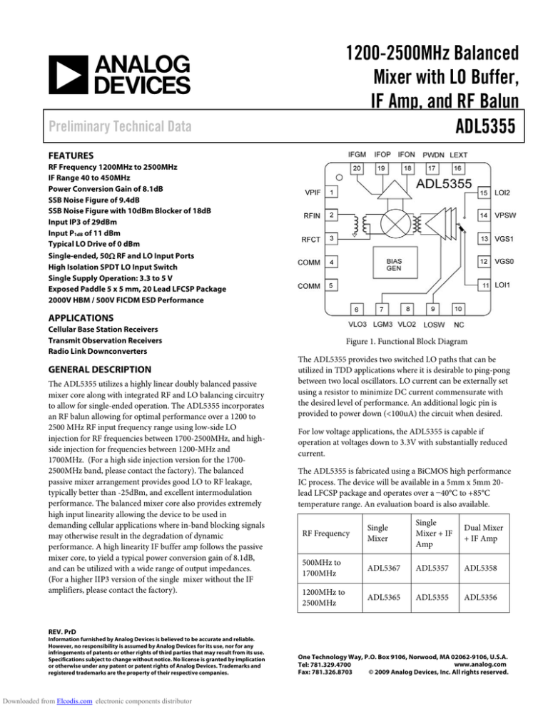
Figure 1. Functional Block Diagram
The ADL5355 provides two switched LO paths that can be
utilized in TDD applications where it is desirable to ping-pong
between two local oscillators. LO current can be externally set
using a resistor to minimize DC current commensurate with
the desired level of performance. An additional logic pin is
provided to power down (<100uA) the circuit when desired.
For low voltage applications, the ADL5355 is capable if
operation at voltages down to 3.3V with substantially reduced
current.
The ADL5355 is fabricated using a BiCMOS high performance
IC process. The device will be available in a 5mm x 5mm 20lead LFCSP package and operates over a −40°C to +85°C
temperature range. An evaluation board is also available.
RF Frequency
Single
Mixer
Single
Mixer + IF
Amp
Dual Mixer
+ IF Amp
500MHz to
1700MHz
ADL5367
ADL5357
ADL5358
1200MHz to
2500MHz
ADL5365
ADL5355
ADL5356
REV. PrD
Information furnished by Analog Devices is believed to be accurate and reliable.
However, no responsibility is assumed by Analog Devices for its use, nor for any
infringements of patents or other rights of third parties that may result from its use.
Specifications subject to change without notice. No license is granted by implication
or otherwise under any patent or patent rights of Analog Devices. Trademarks and
registered trademarks are the property of their respective companies.
Downloaded from Elcodis.com electronic components distributor
One Technology Way, P.O. Box 9106, Norwood, MA 02062-9106, U.S.A.
www.analog.com
Tel: 781.329.4700
Fax: 781.326.8703
© 2009 Analog Devices, Inc. All rights reserved.
ADL5355
Preliminary Technical Data
ADL5355—Specifications
Table 1. VS = 5 V, TA = 25°C, fRF = 1900 MHz, fLO = 1697 MHz, LO power = 0 dBm, Zo = 50Ω, unless otherwise noted
Parameter
Conditions
Min
Typ
Max
Unit
RF INPUT INTERFACE
Return Loss
Tunable to >20dB over a limited bandwidth
Input Impedance
Differential impedance, f = 200 MHz
Ω
2500
450
Externally generated
VS
-3
Low or High Side LO injection
MHz
Ω
200
MHz
V
0
14
50
Input Impedance
LO Frequency Range
50
40
IF Frequency Range
DC Bias Voltage1
LO INTERFACE
LO Power
Return Loss
dB
1200
RF Frequency Range
OUTPUT INTERFACE
Output Impedance
10
1300
+10
dBm
dB
Ω
2200
MHz
DYNAMIC PERFORMANCE
Power Conversion Gain
Including 4:1 IF port transformer and PCB loss
8.1
dB
Voltage Conversion Gain
ZSOURCE = 50Ω, Differential ZLOAD = 200Ω
Differential
14.4
dB
9.4
dB
SSB Noise Figure
SSB Noise Figure Under-Blocking
10dBm Blocker present +/-5MHz from wanted RF
input, LO source filtered
18
dB
Input Third Order Intercept
fRF1 = 1900 MHz, fRF2 = 1901 MHz, fLO = 1697 MHz,
each RF tone at -10 dBm
29
dBm
Input Second Order Intercept
fRF1 = 1900 MHz, fRF2 = 1950 MHz, fLO = 1697 MHz,
each RF tone at -10 dBm
52.5
dBm
11
dBm
-17
dBm
LO to RF Input Leakage
-38
dBm
RF to IF Output Isolation
39
dB
Input 1 dB Compression Point
LO to IF Output Leakage
Unfiltered IF Output
IF/2 Spurious
-10 dBm Input Power
-69
dBc
IF/3 Spurious
-10dBm Input Power
-72
dBc
POWER INTERFACE
Supply Voltage
Quiescent Current
1
3.3
Resistor Programmable
Supply voltage must be applied from external circuit through choke inductors
REV. PrD | Page 2 of 9
Downloaded from Elcodis.com electronic components distributor
5
190
5.5
V
mA
Preliminary Technical Data
ADL5355
ADL5355—Specifications at VS=3.3V
Table 2. VS = 3.3 V, TA = 25°C, fRF = 1900 MHz, fLO = 1697 MHz, LO power = 0 dBm, Zo = 50Ω, unless otherwise noted
Parameter
Conditions
Min
Typ
Max
Unit
DYNAMIC PERFORMANCE
Power Conversion Gain
Including 4:1 IF port transformer and PCB loss
8.7
dB
Voltage Conversion Gain
ZSOURCE = 50Ω, Differential ZLOAD = 200Ω
Differential
15.2
dB
SSB Noise Figure
Including 4:1 IF port transformer and PCB loss
8.9
dB
Input Third Order Intercept
fRF1 = 1899.5 MHz, fRF2 = 1900.5 MHz, fLO = 1697
MHz, each RF tone at -10 dBm
20
dBm
Input Second Order Intercept
fRF1 = 1900 MHz, fRF2 = 1850 MHz, fLO = 1697 MHz,
each RF tone at -10 dBm
50
dBm
7
dBm
Input 1 dB Compression Point
POWER INTERFACE
Supply Voltage
Quiescent Current
3.0
Resistor Programmable
REV. PrD | Page 3 of 9
Downloaded from Elcodis.com electronic components distributor
3.3
120
3.6
V
mA
ADL5355
Preliminary Technical Data
ABSOLUTE MAXIMUM RATINGS
Table 2.
Parameter
Supply Voltage, VPOS
PWDN, LOSW, VGS0, VGS1
RF Input Power RFIN
Internal Power Dissipation
θJA (Exposed Paddle Soldered Down)
θJC (At Exposed Paddle)
Maximum Junction Temperature
Operating Temperature Range
Storage Temperature Range
Rating
5.5 V
TBD
TBD
TBD
TBD
TBD
TBD
−40°C to +85°C
−65°C to +150°C
Stresses above those listed under Absolute Maximum Ratings
may cause permanent damage to the device. This is a stress
rating only; functional operation of the device at these or any
other conditions above those indicated in the operational
section of this specification is not implied. Exposure to absolute
maximum rating conditions for extended periods may affect
device reliability.
ESD CAUTION
REV. PrD | Page 4 of 9
Downloaded from Elcodis.com electronic components distributor
Preliminary Technical Data
ADL5355
PIN CONFIGURATION AND FUNCTION DESCRIPTIONS
Figure 2. Pin Configuration
Table 3. Pin Function Descriptions
Pin No.
1
2
3
4, 5
6, 8
7
9
10
11, 15
12, 13
14
16
17
18, 19
20
Mnemonic
VPIF
RFIN
RFCT
COMM
VLO3, VLO2
LGM3
LOSW
NC
LOI1, LOI2
VGS0, VGS1
VPSW
LEXT
PWDN
IFON, IFOP
IFGM
Function
Positive Supply Voltage for IF Amplifier: 5.00 V.
RF Input. Must be ac-coupled.
RF Balun Center Tap (AC Ground).
Device Common (DC Ground).
Positive Supply Voltage for LO Amplifier.
LO Amplifier Bias Control.
LO Switch.
No Connect.
LO Input. Must be ac-coupled.
Mixer Gate Bias Control. Ground for nominal operation.
Positive Supply Voltage for LO Switch.
IF Return (Ground).
Connect to Ground for Normal Operation. Connect pin to 3.3V for disable mode.
Differential IF output (Open Collectors). Each requires DC bias of 5.00 V (Nominal).
IF Amplifier Bias Control.
REV. PrD | Page 5 of 9
Downloaded from Elcodis.com electronic components distributor
ADL5355
Preliminary Technical Data
TYPICAL PERFORMANCE CHARACTERISTICS
VS = 5 V, TA = 25°C, as measured using typical circuit schematic with low-side LO unless otherwise noted.
15
14
14
13
SSB Noise Figure (dB)
Gain (dB)
12
10
8
6
12
11
10
9
8
7
4
6
2
1500
1600
1700
1800
1900
2000
2100
2200
2300
2400
5
1500
2500
1600
1700
1800
-20
40
-25
LO to RF Leakage (dBm)
45
Input IP3 (dBm)
35
30
25
20
15
1600
1700
1800
1900
2000
2100
2200
2300
2400
2500
2200
2300
2400
2500
2400
2500
-30
-35
-40
-45
-50
15
14
13
12
11
10
9
8
7
6
1700
1800
1900
2000
2100
1600
1700
1800
1900
2000
2100
2200
2300
Figure 7. LO to RF Leakage versus LO Frequency
Figure 4. IIP3 versus RF Frequency
1600
-60
1500
RF Freq (MHz)
RF Freq (MHz)
Input P1dB (dBm)
2100
-55
10
5
1500
2000
Figure 6. Single-Sideband NF versus RF Frequency
Figure 3. Conversion Gain versus RF Frequency
5
1500
1900
RF Frequency (MHz)
RF Freq (MHz)
2200
2300
2400
2500
RF Freq (MHz)
Figure 5. IP1dB versus RF Frequency
REV. PrD | Page 6 of 9
Downloaded from Elcodis.com electronic components distributor
Preliminary Data
ADL5355
EVALUATION BOARD
An evaluation board is available for the family of double balanced mixers, including ADL5355 and ADL5357. The standard evaluation
board schematic is presented in Figure 8. The evaluation board is fabricated on a multilayer Rogers board. Table 4 details the various
configuration options of the evaluation board.
Figure 8. Evaluation Board Schematic.
Table 4. Eval Board Configuration
Components
C2, C6, C8, C18, C19, C20,
C21
Function
Power Supply Decoupling. Nominal supply decoupling consists a 10
μF capacitor to ground in parallel with 10pF capacitors to ground
positioned as close to the device as possible.
C1, C4, C5
RF Input Interface. The input channels is ac-coupled through C1. C4
and C5 provide bypassing for the center taps of the RF input baluns.
REV. PrD | Page 7 of 9
Downloaded from Elcodis.com electronic components distributor
Default Conditions
C2 = 10 μF (size 0603)
C6, C8, C20, C21 = 10 pF (size 0402)
C18, C19 = 100 pF (size 0402)
C1 = 22 pF (size 0402)
C4 = 10 pF (size 0402)
C5 = 0.01 μF (size 0402)
ADL5355
T1, C17, L4, L5, R1, R24,
R25
C10, C12, R4
R21
C22, L3, R9, R14, R22, R23,
VGS0, VGS1
Preliminary Technical Data
IF Output Interface. The open collector IF output interfaces are
biased through pull-up choke inductors L4 and L5. T1is a 4:1
impedance transformer used to provide a single ended IF output
interface, with C17 providing center-tap bypassing. R1 should be
removed for balanced output operation.
LO Interface. C10 and C12 provide ac-coupling for the LO1_IN and
LO2_IN local oscillator inputs. LOSEL selects the appropriate LO
input for both mixer cores. R4 provides a pull-down to ensure
LO1_IN is enabled when the LOSEL test point has logic low. LO2_IN
is enabled when LOSEL is pulled to logic high.
PWDN Interface. R21 pulls the PWDN logic low and enables the
device. PWR_UP test point allows PWDN interface to be excercised
using external logic generator. It is permissible to ground the PWDN
pin for nominal operation.
Bias Control. R22 and R23 form a voltage divider to provide a 3V for
logic control, bypassed to ground through C22. VGS0 and VGS1
jumpers provide programmability at pin VGS0 and VGS1. It is
recommeded to pull these two pins to ground for nominal
operation. R9 sets the bias point for the internal LO buffers. R14 sets
the bias point for the internal IF amplifiers.
REV. PrD | Page 8 of 9
Downloaded from Elcodis.com electronic components distributor
C17 = 150 pF (size 0402)
T1 = TC4-1W+ (MiniCircuits)
L4, L5 = 470 nH (size 1008)
R1, R24, R25 = 0 Ω (size 0402)
C10, C12 = 22pF (size 0402)
R4 = 10kΩ (size 0402)
R21 = 10kΩ (size 0402)
C22 = 1 nF (size 0402)
L3 = 0 Ω (size 0603)
R9 = 1.1 kΩ (size 0402)
R14 = 910 Ω (size 0402)
R22 = 10kΩ (size 0402)
R23 = 15kΩ (size 0402)
VGS0 = VGS1 = 3-pin shunt
Preliminary Technical Data
ADL5355
OUTLINE DIMENSIONS
Figure 9. 20-Lead Lead Frame Chip Scale Package [LFCSP_VQ]
5 mm × 5 mm Body, Very Thin Quad (CP-20-5))
Dimensions shown in millimeters
ORDERING GUIDE
Models
ADL5355XCPZ-R71
ADL5355-EVALZ
1
Temperature
Range
−40°C to +85°C
Package Description
20-Lead Lead Frame Chip Scale Package [LFCSP_VQ]
Evaluation Board
Package
Option
CP-20-5
Branding
TBD
Transport
Media Quantity
TBD, Reel
1
Z = Pb-free part.
REV. PrD | Page 9 of 9
Downloaded from Elcodis.com electronic components distributor
PR08080-0-3/09(PrD)


