DS90LV110AT 1 to 10 LVDS Data/Clock
DS90LV110AT www.ti.com
SNOSAC2J – AUGUST 2004 – REVISED APRIL 2013
DS90LV110AT 1 to 10 LVDS Data/Clock Distributor with Failsafe
Check for Samples: DS90LV110AT
1
FEATURES
2
• Low jitter 400 Mbps fully differential data path
• 145 ps (typ) of pk-pk jitter with PRBS = 2
23
− 1 data pattern at 400 Mbps
• Single +3.3 V Supply
• Balanced output impedance
• Output channel-to-channel skew is 35ps (typ)
• Differential output voltage (V
OD
) is 320mV (typ) with 100 Ω termination load.
• LVDS receiver inputs accept LVPECL signals
• LVDS input failsafe
• Fast propagation delay of 2.8 ns (typ)
• Receiver open, shorted, and terminated input failsafe
• 28 lead TSSOP package
• Conforms to ANSI/TIA/EIA-644 LVDS standard
DESCRIPTION
DS90LV110A is a 1 to 10 data/clock distributor utilizing LVDS (Low Voltage Differential Signaling) technology for low power, high speed operation. Data paths are fully differential from input to output for low noise generation and low pulse width distortion. The design allows connection of 1 input to all 10 outputs.
LVDS I/O enable high speed data transmission for point-to-point interconnects. This device can be used as a high speed differential 1 to 10 signal distribution
/ fanout replacing multi-drop bus applications for higher speed links with improved signal quality. It can also be used for clock distribution up to 200MHz.
The DS90LV110A accepts LVDS signal levels,
LVPECL levels directly or PECL with attenuation networks.
The LVDS outputs can be put into TRI-STATE by use of the enable pin.
For more details, please refer to the
section of this datasheet.
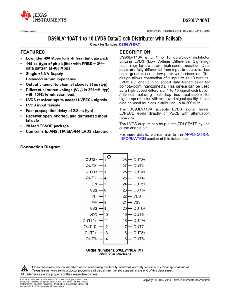
Connection Diagram
Order Number DS90LV110ATMT
PW0028A Package
1
Please be aware that an important notice concerning availability, standard warranty, and use in critical applications of
Texas Instruments semiconductor products and disclaimers thereto appears at the end of this data sheet.
2
All trademarks are the property of their respective owners.
PRODUCTION DATA information is current as of publication date.
Products conform to specifications per the terms of the Texas
Instruments standard warranty. Production processing does not necessarily include testing of all parameters.
Copyright © 2004–2013, Texas Instruments Incorporated
DS90LV110AT
SNOSAC2J – AUGUST 2004 – REVISED APRIL 2013
Block Diagram
www.ti.com
These devices have limited built-in ESD protection. The leads should be shorted together or the device placed in conductive foam during storage or handling to prevent electrostatic damage to the MOS gates.
Absolute Maximum Ratings
(1)
Supply Voltage (V
DD
-V
SS
)
LVCMOS/LVTTL Input Voltage (EN)
LVDS Receiver Input Voltage (IN+, IN − )
LVDS Driver Output Voltage (OUT+, OUT − )
Junction Temperature
Storage Temperature Range
Lead Temperature (Soldering, 4 sec.)
Maximum Package Power
Dissipation at 25°C
28 Lead TSSOP
Package Derating
θ
JA
(4-Layer, 2 oz. Cu, JEDEC)
28 Lead TSSOP
28 Lead TSSOP
ESD Rating:
(HBM, 1.5k
Ω , 100pF)
(EIAJ, 0 Ω , 200pF)
− 0.3V to +4V
− 0.3V to (V
CC
+ 0.3V)
− 0.3V to +4V
− 0.3V to +4V
+150°C
− 65°C to +150°C
+260°C
2.115 W
16.9 mW/°C above +25°C
59.1 °C/W
> 8 kV
> 250 V
(1) “Absolute Maximum Ratings” are these beyond which the safety of the device cannot be verified. They are not meant to imply that the device should be operated at these limits. The table of “Electrical Characteristics” provides conditions for actual device operation.
Recommended Operating Conditions
Supply Voltage (V
DD
- V
SS
)
Receiver Input Voltage
Operating Free Air Temperature
Min
3.0
0
-40
Typ
3.3
+25
Max
3.6
V
DD
+85
Units
V
V
°C
2 Submit Documentation Feedback
Product Folder Links: DS90LV110AT
Copyright © 2004–2013, Texas Instruments Incorporated
DS90LV110AT www.ti.com
SNOSAC2J – AUGUST 2004 – REVISED APRIL 2013
Electrical Characteristics
Over recommended operating supply and temperature ranges unless otherwise specified
Symbol Parameter
LVCMOS/LVTTL DC SPECIFICATIONS (EN)
Conditions Min Typ
(1)
V
IH
V
IL
I
IH
High Level Input Voltage
Low Level Input Voltage
2.0
V
SS
High Level Input Current V
IN
= 3.6V or 2.0V; V
DD
= 3.6V
±7
I
IL
V
CL
Low Level Input Current
Input Clamp Voltage I
V
IN
CL
= 0V or 0.8V; V
DD
= − 18 mA
= 3.6V
LVDS OUTPUT DC SPECIFICATIONS (OUT1, OUT2, OUT3, OUT4, OUT5, OUT6, OUT7, OUT8, OUT9, OUT10)
±7
− 0.8
250
260
320
320
I
V
OD
Differential Output Voltage R
L
= 100 Ω
R
L
= 100 Ω , V
DD
= 3.3V, T
A
= 25°C
I
Δ V
OD
V
OS
Δ V
OZ
OS
I
OFF
Change in V
OD
Offset Voltage between Complimentary Output States
(2)
Change in V
OS between Complimentary Output States
Output TRI-STATE Current EN = 0V,
V
OUT
= V
DD or GND
Power-Off Leakage Current
I
SA
,I
I
SAB
SB
Output Short Circuit Current
Both Outputs Shorted
(3)
LVDS RECEIVER DC SPECIFICATIONS (IN)
V
DD
= 0V; V
OUT
= 3.6V or GND
V
OUT+
OR V
OUT −
= 0V or V
DD
V
OUT+
= V
OUT −
V
V
TH
TL
V
CMR
I
IN
Differential Input High Threshold
Differential Input Low Threshold
Common Mode Voltage Range
Input Current
V
CM
V
DD
= +0.05V or +1.2V or +3.25V,
= 3.3V
V
ID
V
IN
= 100mV, V
DD
= +3.0V, V
DD
= 3.3V
= 3.6V or 0V
V
IN
= 0V, V
DD
= 3.6V or 0V
I
SUPPLY CURRENT
CCD
Total Supply Current R
L
= 100 Ω
EN = High
, C
L
= 5 pF, 200 MHz,
CCZ
TRI-STATE Supply Current
No Load, 200 MHz, EN = High
EN = Low
1.125
− 100
0.05
1.25
±1
±1
12
6
0
0
±1
±1
125
80
15
(1) All typical are given for V
CC
(2) V
OS is defined as (V
OH
+ V
= +3.3V and T
OL
) / 2.
A
= +25°C, unless otherwise stated.
(3) Only one output can be shorted at a time. Don't exceed the package absolute maximum rating.
Max
450
425
35
1.375
35
±10
±10
24
12
V
DD
0.8
±20
±20
− 1.5
+100
3.25
±10
±10
160
125
29
Units mV mV
V
μ A
μ A
V
V
μ A
μ A
V mA mA mA mV mV
|mV|
V
|mV|
μ A
μ A
|mA|
|mA|
Copyright © 2004–2013, Texas Instruments Incorporated
Product Folder Links: DS90LV110AT
Submit Documentation Feedback 3
DS90LV110AT
SNOSAC2J – AUGUST 2004 – REVISED APRIL 2013
AC Electrical Characteristics
T
PLHD
T
PHLD
T
SKEW
T
CCS
T
PHZ
T
PLZ
T
PZH
T
PZL
Over recommended operating supply and temperature ranges unless otherwise specified.
Symbol
T
LHT
T
HLT
T
DJ
T
RJ
Parameter
Output Low-to-High Transition Time, 20% to 80%,
(1)
Conditions
Output High-to-Low Transition Time, 80% to 20%,
(1)
LVDS Data Jitter, Deterministic (Peak-to-
Peak)
(2)
V
ID
V
CM
= 300mV; PRBS=2
23
-1 data;
= 1.2V at 400 Mbps (NRZ)
LVDS Clock Jitter, Random
(2)
V
ID
V
CM
= 300mV;
= 1.2V at 200 MHz clock
Propagation Low to High Delay,
Propagation High to Low Delay,
Pulse Skew |T
PLHD
- T
PHLD
|
(1)
Output Channel-to-Channel Skew,
(1)
Disable Time (Active to TRI-STATE) High to Z,
Disable Time (Active to TRI-STATE) Low to Z,
Enable Time (TRI-STATE to Active) Z to High,
Enable Time (TRI-STATE to Active) Z to Low,
Min
2.2
2.2
Typ
390
390
145
2.8
2.8
2.8
20
35
3.0
1.8
10.0
7.0
Max
550
550
3.6
3.9
340
91
6.0
6.0
23.0
23.0
www.ti.com
Units ps ps ps ps
(1) The parameters are specified by design. The limits are based on statistical analysis of the device performance over PVT (process, voltage and temperature) range.
(2) The measurement used the following equipment and test setup: HP8133A pattern/pulse generator), 5 feet of RG-142 cable with DUT test board and HP83480A (digital scope mainframe) with HP83484A (50GHz scope module). The HP8133A with the RG-142 cable exhibit a T
DJ
= 26ps and T
RJ
= 1.3 ps
AC TIMING DIAGRAMS
ns ns ps ps ns ns ns ns
Figure 1. Output active to TRI-STATE and TRI-STATE to active output time
4 Submit Documentation Feedback
Product Folder Links: DS90LV110AT
Copyright © 2004–2013, Texas Instruments Incorporated
DS90LV110AT
SNOSAC2J – AUGUST 2004 – REVISED APRIL 2013 www.ti.com
Figure 2. LVDS Driver TRI-STATE Circuit
Figure 3. LVDS Output Load
Figure 4. LVDS Output Transition Time
Figure 5. Propagation Delay Low-to-High and High-to-Low
Copyright © 2004–2013, Texas Instruments Incorporated
Product Folder Links: DS90LV110AT
Submit Documentation Feedback 5
DS90LV110AT
SNOSAC2J – AUGUST 2004 – REVISED APRIL 2013 www.ti.com
Figure 6. Output 1 to 10 Channel-to-Channel Skew
APPLICATION INFORMATION
INPUT FAIL-SAFE
The receiver inputs of the DS90LV110A have internal fail-safe biasing for short, open, and teminated input conditions.
LVDS INPUTS TERMINATION
The LVDS Receiver input must have a 100 Ω termination resistor placed as close as possible across the input pins.
UNUSED CONTROL INPUTS
The EN control input pin has internal pull down device. If left open, the 10 outputs will default to TRI-STATE.
EXPANDING THE NUMBER OF OUTPUT PORTS
To expand the number of output ports, more than one DS90LV110A can be used. Total propagation delay through the devices should be considered to determine the maximum expansion. Adding more devices will increase the output jitter due to each pass.
PCB LAYOUT AND POWER SYSTEM BYPASS
Circuit board layout and stack-up for the DS90LV110A should be designed to provide noise-free power to the device. Good layout practice also will separate high frequency or high level inputs and outputs to minimize unwanted stray noise pickup, feedback and interference. Power system performance may be greatly improved by using thin dielectrics (4 to 10 mils) for power/ground sandwiches. This increases the intrinsic capacitance of the
PCB power system which improves power supply filtering, especially at high frequencies, and makes the value and placement of external bypass capacitors less critical. External bypass capacitors should include both RF ceramic and tantalum electrolytic types. RF capacitors may use values in the range 0.01 µF to 0.1 µF. Tantalum capacitors may be in the range 2.2 µF to 10 µF. Voltage rating for tantalum capacitors should be at least 5X the power supply voltage being used. It is recommended practice to use two vias at each power pin of the
DS90LV110A as well as all RF bypass capacitor terminals. Dual vias reduce the interconnect inductance by up to half, thereby reducing interconnect inductance and extending the effective frequency range of the bypass components.
The outer layers of the PCB may be flooded with additional ground plane. These planes will improve shielding and isolation as well as increase the intrinsic capacitance of the power supply plane system. Naturally, to be effective, these planes must be tied to the ground supply plane at frequent intervals with vias. Frequent via placement also improves signal integrity on signal transmission lines by providing short paths for image currents which reduces signal distortion. The planes should be pulled back from all transmission lines and component mounting pads a distance equal to the width of the widest transmission line or the thickness of the dielectric separating the transmission line from the internal power or ground plane(s) whichever is greater. Doing so minimizes effects on transmission line impedances and reduces unwanted parasitic capacitances at component mounting pads.
6 Submit Documentation Feedback
Product Folder Links: DS90LV110AT
Copyright © 2004–2013, Texas Instruments Incorporated
DS90LV110AT www.ti.com
SNOSAC2J – AUGUST 2004 – REVISED APRIL 2013
There are more common practices which should be followed when designing PCBs for LVDS signaling. Please see Application Note: AN-1108( SNLA008 ) for additional information.
INPUT INTERFACING
The DS90LV110A accepts differential signals and allow simple AC or DC coupling. With a wide common mode range, the DS90LV110A can be DC-coupled with all common differential drivers (that is, LVPECL, LVDS, CML).
,
, and
illustrate typical DC-coupled interface to common differential drivers.
LVDS
Driver
DS90LV110A
Receiver
OUT+
100 : Differential T-Line
IN+
100 :
IN-
OUT-
Figure 7. Typical LVDS Driver DC-Coupled Interface to DS90LV110A Input
CML3.3V or CML2.5V
Driver
V
CC
DS90LV110A
Receiver
50 : 50 :
100 : Differential T-Line
100 :
IN-
OUT-
Figure 8. Typical CML Driver DC-Coupled Interface to DS90LV110A Input
LVPECL
Driver
OUT+
OUT+
100 : Differential T-Line
IN+
IN+
DS90LV110A
Receiver
100 :
IN-
OUT-
50 : 50 :
Figure 9. Typical LVPECL Driver DC-Coupled Interface to DS90LV110A Input
Copyright © 2004–2013, Texas Instruments Incorporated
Product Folder Links: DS90LV110AT
Submit Documentation Feedback 7
DS90LV110AT
SNOSAC2J – AUGUST 2004 – REVISED APRIL 2013 www.ti.com
OUTPUT INTERFACING
The DS90LV110A outputs signals that are compliant to the LVDS standard. Their outputs can be DC-coupled to most common differential receivers.
illustrates typical DC-coupled interface to common differential receivers and assumes that the receivers have high impedance inputs. While most differential receivers have a common mode input range that can accommodate LVDS compliant signals, it is recommended to check respective receiver's data sheet prior to implementing the suggested interface implementation.
DS90LV110A
Driver
OUT+
100 : Differential T-Line
IN+
Differential
Receiver
100 :
CML or
LVPECL or
LVDS
IN-
OUT-
Figure 10. Typical DS90LV110A Output DC-Coupled Interface to an LVDS, CML or LVPECL Receiver
Pin Name
IN+
IN -
OUT+
OUT -
EN
V
SS
V
DD
# of Pin
1
1
10
10
1
3
2
DS90LV110A PIN DESCRIPTIONS
Input/Output
I Non-inverting LVDS input
P
P
O
I
I
O
Description
Inverting LVDS input
Non-inverting LVDS Output
Inverting LVDS Output
This pin has an internal pull-down when left open. A logic low on the
Enable puts all the LVDS outputs into TRI-STATE and reduces the supply current.
Ground (all ground pins must be tied to the same supply)
Power Supply (all power pins must be tied to the same supply)
8 Submit Documentation Feedback
Product Folder Links: DS90LV110AT
Copyright © 2004–2013, Texas Instruments Incorporated
www.ti.com
MULTI-DROP APPLICATIONS
DS90LV110AT
SNOSAC2J – AUGUST 2004 – REVISED APRIL 2013
POINT-TO-POINT DISTRIBUTION APPLICATIONS
For applications operating at data rate greater than 400Mbps, a point-to-point distribution application should be used. This improves signal quality compared to multi-drop applications due to no stub PCB trace loading. The only load is a receiver at the far end of the transmission line. Point-to-point distribution applications will have a wider LVDS bus lines, but data rate can increase well above 400Mbps due to the improved signal quality.
Copyright © 2004–2013, Texas Instruments Incorporated
Product Folder Links: DS90LV110AT
Submit Documentation Feedback 9
DS90LV110AT
SNOSAC2J – AUGUST 2004 – REVISED APRIL 2013 www.ti.com
Typical Performance Characteristics
Output Voltage (V
OD
) vs. Resistive Load (R
L
) Peak-to-Peak Output Jitter at V
CM
= +0.4V vs. VID
Peak-to-Peak Output Jitter at V
CM
= +1.2V vs. VID Peak-to-Peak Output Jitter at V
CM
= +2.9V vs. VID
10 Submit Documentation Feedback
Product Folder Links: DS90LV110AT
Copyright © 2004–2013, Texas Instruments Incorporated
DS90LV110AT www.ti.com
SNOSAC2J – AUGUST 2004 – REVISED APRIL 2013
REVISION HISTORY
Changes from Revision I (April 2013) to Revision J Page
• Changed layout of National Data Sheet to TI format ............................................................................................................
Copyright © 2004–2013, Texas Instruments Incorporated
Product Folder Links: DS90LV110AT
Submit Documentation Feedback 11
PACKAGE OPTION ADDENDUM www.ti.com
13-Sep-2014
PACKAGING INFORMATION
Orderable Device
DS90LV110ATMT
Status
(1)
NRND
Package Type Package
Drawing
Pins Package
Qty
TSSOP PW 28 48
Eco Plan
(2)
TBD
Lead/Ball Finish
(6)
Call TI
MSL Peak Temp
(3)
Call TI
Op Temp (°C)
-40 to 85
Device Marking
(4/5)
DS90LV
110ATMT
DS90LV
110ATMT
DS90LV110ATMT/NOPB ACTIVE TSSOP PW 28 48 Green (RoHS
& no Sb/Br)
CU SN Level-3-260C-168 HR -40 to 85
DS90LV110ATMTX/NOPB ACTIVE TSSOP PW 28 2500 Green (RoHS
& no Sb/Br)
CU SN Level-3-260C-168 HR
(1)
The marketing status values are defined as follows:
ACTIVE: Product device recommended for new designs.
LIFEBUY: TI has announced that the device will be discontinued, and a lifetime-buy period is in effect.
NRND: Not recommended for new designs. Device is in production to support existing customers, but TI does not recommend using this part in a new design.
PREVIEW: Device has been announced but is not in production. Samples may or may not be available.
OBSOLETE: TI has discontinued the production of the device.
-40 to 85 DS90LV
110ATMT
(2)
Eco Plan - The planned eco-friendly classification: Pb-Free (RoHS), Pb-Free (RoHS Exempt), or Green (RoHS & no Sb/Br) - please check http://www.ti.com/productcontent for the latest availability information and additional product content details.
TBD: The Pb-Free/Green conversion plan has not been defined.
Pb-Free (RoHS): TI's terms "Lead-Free" or "Pb-Free" mean semiconductor products that are compatible with the current RoHS requirements for all 6 substances, including the requirement that lead not exceed 0.1% by weight in homogeneous materials. Where designed to be soldered at high temperatures, TI Pb-Free products are suitable for use in specified lead-free processes.
Pb-Free (RoHS Exempt): This component has a RoHS exemption for either 1) lead-based flip-chip solder bumps used between the die and package, or 2) lead-based die adhesive used between the die and leadframe. The component is otherwise considered Pb-Free (RoHS compatible) as defined above.
Green (RoHS & no Sb/Br): TI defines "Green" to mean Pb-Free (RoHS compatible), and free of Bromine (Br) and Antimony (Sb) based flame retardants (Br or Sb do not exceed 0.1% by weight in homogeneous material)
(3)
MSL, Peak Temp. - The Moisture Sensitivity Level rating according to the JEDEC industry standard classifications, and peak solder temperature.
(4)
There may be additional marking, which relates to the logo, the lot trace code information, or the environmental category on the device.
(5)
Multiple Device Markings will be inside parentheses. Only one Device Marking contained in parentheses and separated by a "~" will appear on a device. If a line is indented then it is a continuation of the previous line and the two combined represent the entire Device Marking for that device.
(6)
Lead/Ball Finish - Orderable Devices may have multiple material finish options. Finish options are separated by a vertical ruled line. Lead/Ball Finish values may wrap to two lines if the finish value exceeds the maximum column width.
Important Information and Disclaimer:The information provided on this page represents TI's knowledge and belief as of the date that it is provided. TI bases its knowledge and belief on information provided by third parties, and makes no representation or warranty as to the accuracy of such information. Efforts are underway to better integrate information from third parties. TI has taken and
Addendum-Page 1
Samples
PACKAGE OPTION ADDENDUM www.ti.com
13-Sep-2014 continues to take reasonable steps to provide representative and accurate information but may not have conducted destructive testing or chemical analysis on incoming materials and chemicals.
TI and TI suppliers consider certain information to be proprietary, and thus CAS numbers and other limited information may not be available for release.
In no event shall TI's liability arising out of such information exceed the total purchase price of the TI part(s) at issue in this document sold by TI to Customer on an annual basis.
Addendum-Page 2
www.ti.com
TAPE AND REEL INFORMATION
PACKAGE MATERIALS INFORMATION
23-Sep-2013
*All dimensions are nominal
Device Package
Type
Package
Drawing
DS90LV110ATMTX/NOPB TSSOP PW
Pins
28
SPQ
2500
Reel
Diameter
(mm)
Reel
Width
W1 (mm)
330.0
16.4
A0
(mm)
6.8
B0
(mm)
10.2
K0
(mm)
P1
(mm)
1.6
8.0
W
(mm)
Pin1
Quadrant
16.0
Q1
Pack Materials-Page 1
www.ti.com
PACKAGE MATERIALS INFORMATION
23-Sep-2013
*All dimensions are nominal
Device
DS90LV110ATMTX/NOPB
Package Type Package Drawing Pins
TSSOP PW 28
SPQ
2500
Length (mm) Width (mm) Height (mm)
367.0
367.0
38.0
Pack Materials-Page 2
IMPORTANT NOTICE
Texas Instruments Incorporated and its subsidiaries (TI) reserve the right to make corrections, enhancements, improvements and other changes to its semiconductor products and services per JESD46, latest issue, and to discontinue any product or service per JESD48, latest issue. Buyers should obtain the latest relevant information before placing orders and should verify that such information is current and complete. All semiconductor products (also referred to herein as “components”) are sold subject to TI’s terms and conditions of sale supplied at the time of order acknowledgment.
TI warrants performance of its components to the specifications applicable at the time of sale, in accordance with the warranty in TI’s terms and conditions of sale of semiconductor products. Testing and other quality control techniques are used to the extent TI deems necessary to support this warranty. Except where mandated by applicable law, testing of all parameters of each component is not necessarily performed.
TI assumes no liability for applications assistance or the design of Buyers’ products. Buyers are responsible for their products and applications using TI components. To minimize the risks associated with Buyers’ products and applications, Buyers should provide adequate design and operating safeguards.
TI does not warrant or represent that any license, either express or implied, is granted under any patent right, copyright, mask work right, or other intellectual property right relating to any combination, machine, or process in which TI components or services are used. Information published by TI regarding third-party products or services does not constitute a license to use such products or services or a warranty or endorsement thereof. Use of such information may require a license from a third party under the patents or other intellectual property of the third party, or a license from TI under the patents or other intellectual property of TI.
Reproduction of significant portions of TI information in TI data books or data sheets is permissible only if reproduction is without alteration and is accompanied by all associated warranties, conditions, limitations, and notices. TI is not responsible or liable for such altered documentation. Information of third parties may be subject to additional restrictions.
Resale of TI components or services with statements different from or beyond the parameters stated by TI for that component or service voids all express and any implied warranties for the associated TI component or service and is an unfair and deceptive business practice.
TI is not responsible or liable for any such statements.
Buyer acknowledges and agrees that it is solely responsible for compliance with all legal, regulatory and safety-related requirements concerning its products, and any use of TI components in its applications, notwithstanding any applications-related information or support that may be provided by TI. Buyer represents and agrees that it has all the necessary expertise to create and implement safeguards which anticipate dangerous consequences of failures, monitor failures and their consequences, lessen the likelihood of failures that might cause harm and take appropriate remedial actions. Buyer will fully indemnify TI and its representatives against any damages arising out of the use of any TI components in safety-critical applications.
In some cases, TI components may be promoted specifically to facilitate safety-related applications. With such components, TI’s goal is to help enable customers to design and create their own end-product solutions that meet applicable functional safety standards and requirements. Nonetheless, such components are subject to these terms.
No TI components are authorized for use in FDA Class III (or similar life-critical medical equipment) unless authorized officers of the parties have executed a special agreement specifically governing such use.
Only those TI components which TI has specifically designated as military grade or “enhanced plastic” are designed and intended for use in military/aerospace applications or environments. Buyer acknowledges and agrees that any military or aerospace use of TI components which have not been so designated is solely at the Buyer's risk, and that Buyer is solely responsible for compliance with all legal and regulatory requirements in connection with such use.
TI has specifically designated certain components as meeting ISO/TS16949 requirements, mainly for automotive use. In any case of use of non-designated products, TI will not be responsible for any failure to meet ISO/TS16949.
Products Applications
Audio
Amplifiers
Data Converters
DLP® Products
DSP
Clocks and Timers
Interface
Logic
Power Mgmt
Microcontrollers
RFID
OMAP Applications Processors
Wireless Connectivity www.ti.com/audio amplifier.ti.com
dataconverter.ti.com
www.dlp.com
dsp.ti.com
www.ti.com/clocks interface.ti.com
logic.ti.com
power.ti.com
microcontroller.ti.com
www.ti-rfid.com
www.ti.com/omap
Automotive and Transportation www.ti.com/automotive
Communications and Telecom www.ti.com/communications
Computers and Peripherals
Consumer Electronics
Energy and Lighting
Industrial
Medical
Security www.ti.com/computers www.ti.com/consumer-apps www.ti.com/energy www.ti.com/industrial www.ti.com/medical www.ti.com/security
Space, Avionics and Defense www.ti.com/space-avionics-defense
Video and Imaging
TI E2E Community www.ti.com/wirelessconnectivity www.ti.com/video e2e.ti.com
Mailing Address: Texas Instruments, Post Office Box 655303, Dallas, Texas 75265
Copyright © 2014, Texas Instruments Incorporated
