Journal of Crystal Growth 136 (1994) 235—240
North-Holland
oo~~ o,
CRYSTAL
GROWTH
Quasi-planar GaAs heterojunction bipolar transistor device entirely
grown by chemical beam epitaxy
F. Alexandre, D. Zerguine, P. Launay, J.L. Benchimol, M. Berz, B. Sermage, D. Komatitsch
and M. Juhel
France Telecom, CNET, Laboratoire de Bagnewc, 196 Avenue Henri Ravera, BP 107, F-92225 Bagneux Cedex, France
Quasi-planar GaAs/GaInP heterojunction bipolar transistor (HBT) structures, fabricated with selective regrowth of an
improved collector contact, are reported. Such devices present a planar surface topology which should allow large scale integration.
The initial growth of the new HBT structure and the selective regrowth of the collector contact are performed by chemical beam
epitaxy (CBE). In the case of the high C base doping level, the high temperature regrowth process induces some degradation of the
HBT current gain which is analysed in terms of a decrease in minority carrier lifetime. Despite this effect, promising microwave
performances are obtained with a cut-off frequency and maximum oscillation frequency of 30 and 25 GHz, respectively.
1. Introduction
Chemical beam epitaxy (CBE) is now recognized as a powerful growth technique for the
realization of GaAs based heterojunction bipolar
transistor (HBT) devices, mainly because of its
capability to produce extremely high and stable
p-type C-doping concentrations in GaAs, using
trimethylgallium (TMG) precursor [1]. In addition, CBE is also the optimum growth technique
for achieving selective area growth, which enables
a three-dimensional control of epitaxial layers.
These additional capabilities expand the flexibility of device and circuit design, and are of great
interest for the simplification of the post-growth
processing of epitaxial device structures and also
the monolithic integration of Ill—V (opto)electronic components using selective growth processes.
In the conventional HBT technology, the wafer
surface is etched back every time a new layer is
accessed in the transistor structure. Consequently, device contacts are present at different
depths from the surface down to typically 1 ~.tm.
The maximum step required for the collector
contact is mainly determined by the thickness of
the collector layer, which is optimized according
to device specifications, such as base—collector
capacitance and breakdown voltage. This results
in a non-planar device structure which is a limitation for the formation of reliable metal interconnections and also for large scale integration.
In the present study, we have investigated a
new HBT epitaxial process entirely based on CBE
of GaAs and related materials, in order to obtain
quasi-planar HBTs. The final surface step height
is reduced to less than 0.3 ~xm by a selective
regrowth of the collector contact on the subcollector layer, the base and emitter surfaces being
covered by a dielectric mask. A direct advantage
of this technological approach is the improvement of the collector contact, since a GaInAs
contact layer can now be grown on top of the
regrown subcollector. Such a contact provides a
low Schottky barrier, which is found to be effective in obtaining very low resistivity ohmic contacts without alloying, in a way similar to that
which has already been realized for the emitter
contact [21. A similar solution has already been
reported for the improvement of the base contact
by a selective CBE regrowth of a heavily C-doped
extrinsic base layer [3]. Thus, in the future, the
0022-0248/94/$07.00 © 1994 — Elsevier Science B.V. All rights reserved
SSDI 0022-0248(93)E0412-Z
236
F. Alexondre ci al.
/
Quasi-planar GaAs HBT device entirely grown by CBE
collector, base and emitter regions could be con
tacted at the surface of the device with the same
contact material such as a refractory tungsten
metal which allows patterning by reactive ion
etching (RIE). This leads to a simplification and
to a higher reliability of the contacting of the
resulting integrated circuits.
The CBE selective growth conditions for this
application have been studied recently [4]. The
present paper is focused on the HBT current gain
degradation observed after the thermal treatment
required for the selective regrowth. This thermal
degradation is analysed in terms of the minority
carrier lifetime in the C-doped GaAs base layer,
measured by photoluminescence decay, and has
been investigated versus C-doping level growth
conditions and annealing temperature in order to
reduce such degradation.
We also report the successful validation of this
technological approach by the measurement of
promising microwave performances of a quasiplanar C-base-doped HBT device produced with
a selectively regrown collector contact.
2. Growth procedure for the quasi-planar HBT
process
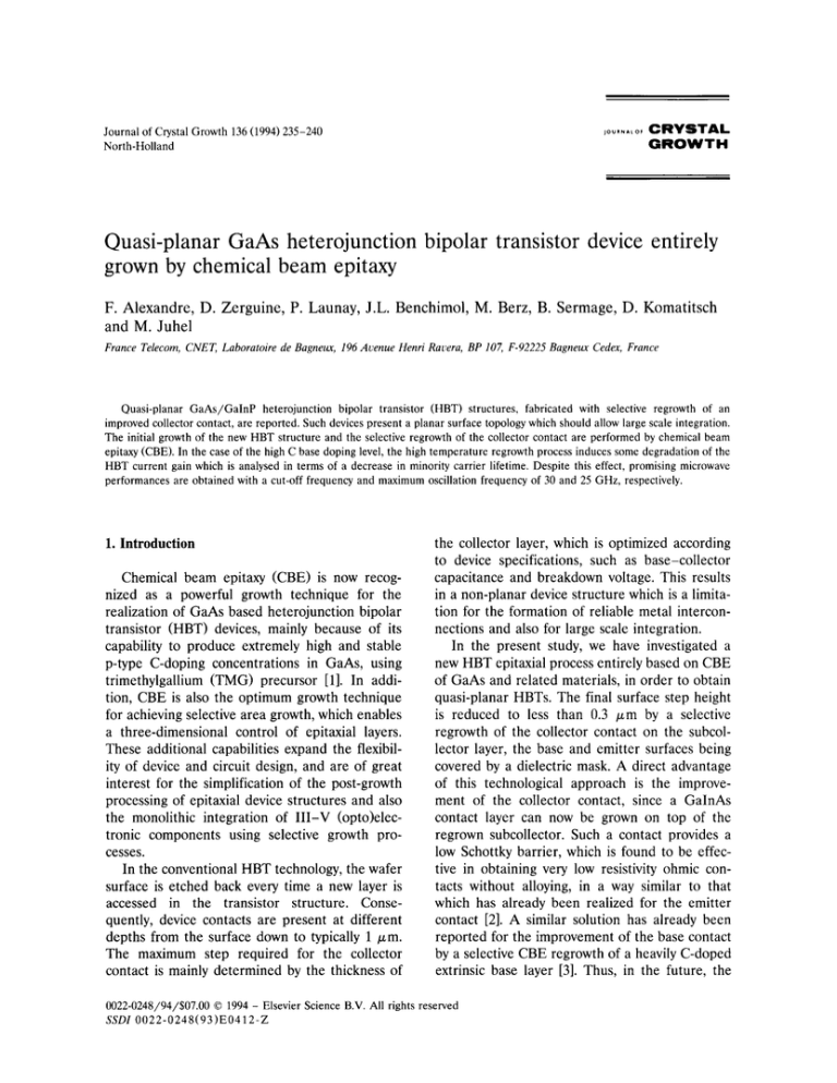
The starting HBT epitaxial structure, described in table 1, is grown by CBE on a (100)
semi-insulating GaAs substrate using conven-
3
50 nm
_______________________________________________
Emitter E
n~-Ga03~
1n
Si: iO’~cm
065As
3
n~-Ga1
In As
Si: 1019 cm
ntGaAs
Si: 2x 1018 cm3
n-GaAIAs
n-GaInP
B
19
.
50 nm
cm
Si: 2X10’6 cm3
Subcollector C
n -GaAs
Si: 2.5>< 10
.
.
170 nm
30 nm
—3
p - a s
n-GaAs
GaAs
SI substrate
50 nm
Si: 4 x io’~cm3
Si: 4X iO~cm3
ase
Collector C
±
Can +
Sidewall
c OiltdC
/
emitter
collector
\ E i/ c
/
B\
/ regrown
~
/.~
,/
.
___________
base
~j
B—H implantation Collector I
*
.
/
B—W implantation
Subcollector
____________
SI substrate
______
Fig. i. Cross-sectional view (a) and SEM surface micrograph
(b) of the final quasi-planar HBT after the collector contact
regrowth process. The marker refers to 5 ~m scale.
tional group V hydrides and group III organometallic sources. The n- and p-type dopants are
provided from solid silicon and trimethylgallium
sources, respectively. A low growth temperature
of 500°C is used for the whole structure. The
HBT has a specific emitter bilayer structure made
of two high-bandgap semiconductors: a 30 nm
thick Ga0 52In0 48P layer is inserted between the
C-doped base layer and the Ga0 7A103As emitter
layer. Among many advantages [5] of this emitter
Table I
HBT initial structure
CapE’
(b)
cm
GaInP and GaAs offers the possibility to contact
the base layer very easily. This overcomes the
main difficulty of the-current HBT technology,
and very good ohmic base contacts are obtained,
even on very thin base layers.
The structure of the selectively regrown collector contact is similar to that of the emitter contact and consists of 1 ~xmthick n~-GaAs(5 x
10i8
3) followed by 100 nm n~tGai X In X As (1
x
cm
10i9 cm 3) with a graded In composition of up to
0.65. Fig. I shows a schematic cross section and a
scanning electron microscope (SEM) view of the
.
nm
490nm
,X
~
.
using
chemical
plasma etching,
between
bilayereither
structure,
theoretching
selectivity,
when
3
510 nm
—
F. Alexandre et al.
/ Quasi-planar GaAs HBT device entirely grown by CBE
quasi-planar HBT. The regrowth regions are previously defined by opening windows in a 1000 A
thick Si3N4 mask deposited on the whole wafer
by plasma enhanced chemical vapour deposition
(PECVD). Then a vertical SiCI4 reactive ion
etching of the HBT structure through the mask
windows is achieved from the emitter cap down
to the subcollector layer. Si3N4 vertical spacers,
deposited by PECVD and etched by reactive ion
etching (RIE), ensure the lateral isolation between the regrown collector contact and the other
HBT active layers. A specific surface preparation,
consisting
of aassisted
100 A ozone
deep chemical
followed
by UV
treatment,etching
and a few
minutes of silicon predeposition prior to the regrowth, are applied in order to minimize the
residual carbon surface contamination and to ensure the nttype continuity at the regrowth interface [4].
The CBE selective regrowth of GaAs and
GaInAs is performed at substrate temperatures
of 650 and 550°C,respectively. A high 2.5 gm/h
GaAs growth rate is used in order to minimize
the time of the thermal treatment corresponding
to the regrowth. With such growth conditions, a
perfect growth selectivity is obtained with absolutely no deposition on the dielectric mask, and
the layer exhibits a high thickness uniformity. A
slight growth rate enhancement (only a few percent of the selective regrowth thickness) is observed only in the vicinity of mask edges, due to
the migration of species from the slow growing
(111) sidewall planes. Furthermore, we have obtamed recently, after optimization of the selective
GaAs growth conditions, vertical sidewalls without lateral overgrowth [10]. These two features,
which are specific to the CBE technique, are
required for the easy removal of the mask and for
the realization of a planar surface.
The final technological steps are the device
isolation by ion implantation, the emitter and
collector contacting by a 3000 A thick tungsten
film, and the C-doped base contacting by Mn—
Au—Ti—Au ohmic contact through the GaInP
layer, after the GaA1As emitter mesa has been
formed by selective etching.
All these different technological steps are realized on 2 inch wafers. For the two CBE growth
237
steps, the wafer is mounted indium-free and
heated radiatively through a boron nitride diffusing plate. The growth temperature is monitored
by an optical pyrometer working at a wavelength
of 0.94 ~m.
3. Static quasi-planar HBT characterization
Transmission line measurements (TLMs) were
used to extract the electrical parameters of the
collector contact regrowth.
A resistivity
2 has been
obtained contact
for a 1 as
fi
low as 10—6
11 cm
contact
resistance.
Static performances have been obtained on
HBTs with a 2 X 15 ~m2 emitter—base junction
area and a 6 x 15 j.tm2 collector—base junction
area. A common emitter current gain (f3) of 2.5
for a base sheet resistance of 140 fl/U was
measured, with a breakdown voltage of the collector—base junction BVCEO above 15 V. This /3
value is low, as compared to the value of 23
measured on a similar HBT structure processed
with a low temperature conventional double-mesa
technology, although the base sheet resistance is
constant within 10%.
This degradation of current gain after the
thermal treatment required for the regrowth process cannot be attributed to a base dopant diffusion towards the emitter layer, as shown by secondary ion mass spectrometry (SIMS). More precisely, the same low value of 1.21 V for the
emitter—base threshold voltage is measured for
both the low temperature conventional HBT
technology and the high temperature technology
with the regrowth process. This threshold voltage,
defined as the emitter—base voltage required to
generate a fixed value of the collector current,
has been found to be extremely sensitive to base
dopant diffusion, and the low measured value
agrees well with a simulation without dopant
diffusion [6]. This behaviour is in accordance with
the high thermal stability of C dopant in GaAs.
In order to determine the origins of the device
performance degradation, we have performed
some measurements by time-resolved photoluminescence, of minority carrier lifetime in C-doped
GaAs layers sandwiched by undoped GaAlAs lay-
238
F. Alexandre et a!.
-
/
Quasi-planar GaAs HBT device entirely grown by CBE
I
•
•
-
I
~
:
I
-
P-S
- * 1018 cm ~3
AG
ANNEALING TEMPERATURE
_______________________________
650
Fig. 2. Electron lifetime in C-doped GaAs layers for two
different C doping levels, as a function of annealing temperalure and also compared to the value in the as-grown (AG)
material. Full circles refer to a 60 mm annealing time and
open circles refer to 15 mm annealing time under cracked
AsH . In this latter case same values are also presented for
annealing under As
4 pressure.
ers. The purpose of the double heterostructure is
to confine induced carriers in the p-type GaAs
layer and to eliminate the influence of surface
recombination. Fig. 2 shows for
doping
3),two
the Cevolution
levels
(5 x 10i8
and as
5 ><compared
10i9 cm to the as-grown
of
electron
lifetime
sample and as a function of annealing temperature (450, 550 and 650°Cfor 1 h and under AsH
3
pressure). The observed behaviour is not drastically changed with a shorter annealing duration
(15 mm) or under a hydrogen free pressure (As4).
The electron lifetime decrease is more pronounced for high C concentrations and also for
high annealing
temperatures.
In the case toofthea
thermal
treatment
at 650°C,corresponding
applied regrowth process used, the same decrease
of about one order of magnitude for a C-doping
level in the mid~10i9cm3 range is found both
for the minority carrier lifetime and for the HBT
current gain. This correlation follows well the
dependence of the current gain /3 with the electron lifetime in the base layer r according to the
relation:
/3
~
~— /
EC’
where TEC is the transit time of electrons from
the emitter to the collector. This demonstrates
that the thermal degradation of the HBT current
gain is directly related to the reduction of minority carrier lifetime after anneal. Similar results on
samples grown by metalorganic chemical vapour
deposition have been found in our own study and
in ref. [7].
To investigate the mechanism causing the minority carrier lifetime change with annealing, the
corresponding variation in concentration of both
carbon with
SIMS,
and detection
hydrogen limits
atomsofwere
I x 1017
measured
and 4 by
x
3,
respectively.
In
the
case
of
C-doping
levels
higher than 5 x 1019 cm3, we can detect a
10i8 cm
hydrogen
content which amounts to more than
10% of the C content in the as-grown layers, and
which decreases drastically to lower than the
SIMS detection limit, after annealing at 650°C.
There has been evidence that hydrogen is incorporated into the C-doped layer along with car.
.
bon, via the incomplete decomposition of
trimethylgallium species [8]. We think therefore
that the reduction of electron lifetime after anneal is related to the exodiffusion of hydrogen
atoms. We speculate that the unstable behaviour
of the already
highly C present
doped layers
be duematerial.
to deep
levels
in themust
as-grown
Such defects might be hydrogen passivated in the
as-grown layer and are then revealed when the
hydrogen is removed during high temperature
thermal treatment [9].
From the present data, it appears that a reduced thermal degradation of the minority carrier properties, compatible with a sufficient HBT
current gain, can be obtained in the case3 ofand
C
doping
concentrations
up to 2 x 10i9lower
cm than
for
selective
regrowthoftemperature
650°C.This critical temperature can be decreased
down to 550°C by using a reduced 0.8 gm/h
selective growth rate when growing with the use
of a triethylgallium (TEG) precursor [10], and
down to 450°Cin the case of a TMG source [11].
In this way, the thermal degradation of HBT
current gain has been reduced to a factor of 2
[12]. Moreover, we have recently succeeded in
obtaining
stableGaAs
minority
carrier
of
heavily quite
C-doped
layers
up toproperties
2 x 10²⁰
cm3 even after high temperature annealing, by
atomic layer epitaxy using the alternative supply
of TMG and arsine [13].
F. Alexandre et al.
/ Quasi-planar GaAs HBT device entirely grown by CBE
4. Microwave quasi-planar HBT characterization
The microwave measurements have been carned out on a Wiltron 360 network analyser. The
S parameters of the HBTs are measured up to 40
GHz. The microwave current and power gains
are displayed in fig. 3, for a current density of
4.5 x iO~ A/cm2 and HBT bias conditions of
VEB 1.5 V and 1/CE 3 V. A cut-off frequency,
F~,of 30 GHz and a maximum oscillation frequency, Fmax, above 25 GHz have been measured. The latter frequency is extrapolated from
the main part of the power gain curve with a —6
dB/octave. These first microwave performances
on the planar HBT devices obtained using the
selective regrowth collector contact are already
comparable with values obtained with a conventional multi-mesa technology.
=
=
239
allows a quasi-planar device to be realized. In the
case of a high temperature regrowth process, and
of C-base doping levels above 2 x 10i9 cm3, a
degradation of the HBT current gain has been
found and has been correlated directly with a
decrease of minority carrier lifetime in the base
layer. It has been proposed that this behaviour
for high C concentrations must be due to deep
centres already present in the as-grown material.
We suggest that these defects are passivated by
the hydrogen present in the as-grown layer and
•are then revealed when hydrogen is removed
during the high temperature thermal treatment.
Despite this effect, promising microwave performances of 30 and 25 GHz for F~ and Fmax,
respectively, have already been obtained.
Acknowledgements
5. Conclusion
In summary, we have presented a new quasiplanar GaAs/GaInP HBT technology. The main
technological step is the selective CBE regrowth
of an improved collector contact from the bottom
subcollector layer up to the emitter layer, which
The authors would like to thank C. Besombes,
A.M. Duchenois, F. Héliot, D. Arquey and L.
Bricard for support in technology and J.P. Médus
for the static and microwave measurements.
References
[1] iL.
Benchimol, F. Alexandre, C. Dubon-Chevallier, F.
Héliot, R. Bourguiba, J. Dangla and B. Sermage, Elec-
25
~
a)
_________________________________________
Letters 28 (1992)
1344. G.D. Petit, T. Jackson and
[21tron.
J.M. Woodhall,
J.L. Freeouf,
MAG
P. Kirchner, J. Vacuum Sci. Technol. 19 (1982) 626.
[3] H. Shimawaki, N. Furuhata, Y. Amamiya and K. Honjo,
in: Gallium Arsenide and Related Compounds 1992,
I
~
I
I
20
\
a
~
15
0
10
.
lh
-
21l
0
2
10
3
10
I
10
I
10
Frequency (MHz)
2 quasiHBTs
versus
Fig. 3. Current planar
gain and
power
gainfrequency.
of the 2x 15 ~cm
Inst. Phys. Conf. Ser. 129, Eds. T. Ikegami, F. Hasegawa
and Y. Takeda (Inst. Phys., Bristol, 1993) 693.
[4] F. Alexandre, D. Zerguine, P. Launay, J.L. Benchimol
and J. Etrillard, J. Crystal Growth 127 (1993) 221.
[51C. Dubon-Chevallier, F. Alexandre, J.L. Benchimol, J.
Dangla, V. Amarger, F. Héliot and R. Bourguiba, Electron. Letters 28 (1992) 2398.
[6] 1. Dangla, C. Dubon-Chevallier, M. Filoche and R.
Azoulay, Electron. Letters 26 (1990) 1061.
[7] U. Strauss, A.P. Heberle, X.Q. Zhou, W.W. RGhle, T.
Lauterbach, KU. Bachen and N.M. Haegel, Japan. J.
AppI. Phys. 32 (1993) 495.
[8] D.M. Kozuch, M. Stavola, S.J. Pearton, C.R. Albernathy
and J. Lapota, AppI. Phys. Letters 57(1990) 2561.
[9] bers,
N. Pan,
Bose, CR.
M.H.Ito
Kim,
F. ChamG. S.S.
Devane,
andG.E.
M. Stillman,
Feng, AppI.
Phys.
Letters 51(1987) 596.
240
F. Alexandre et a!.
/
Quasi-planar GaAs HBT device entirely grown by CBE
[10] P. Legay, F. Alexandre, M. Nunez, J. Sapriel, D. Zerguine and J.L. Benchimol, to be published.
[11] N. Furukawa, H. Shimawaki and A. Okamoto, J. Crystal
Growth 107 (1991) 1049.
[12] D. Zerguine, F. Alexandre, P. Launay, P. Legay, iL.
Benchimol and R. Driad, in: GaAs and Related Compounds 1993, Inst. Phys. Conf. Ser. (Inst. Phys., Bristol, in
press).
[13] MW. Berz, F. Alexandre, J.L. Benchimol, M. Juhel, B.
Sermage and G. Leroux, to be published.


