AN3111
Rev 5, 04/2010
Freescale Semiconductor
Application Note
Soldering the QFN Stacked Die Sensors to a
PC Board
by: Thomas Koschmieder, Cheol Han, Kimberly Tuck, John Dixon
Sensor and Actuator Solutions Division
Tempe, Arizona
INTRODUCTION
The purpose of this application note is to describe
suggested methods of soldering sensor QFN devices to a
Printed Circuit Board (PCB) for both automotive and
consumer applications. Actual experience and surface mount
development efforts are required to optimize the process per
individual device requirements and practices.
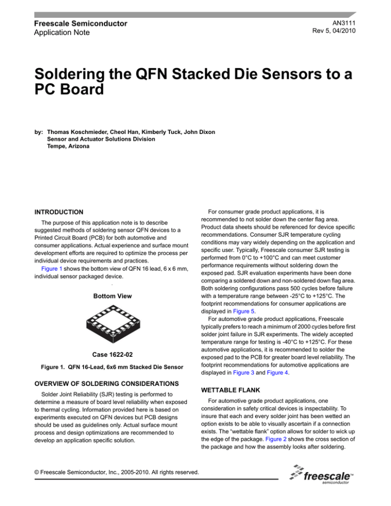
Figure 1 shows the bottom view of QFN 16 lead, 6 x 6 mm,
individual sensor packaged device.
.
Bottom View
Case 1622-02
Figure 1. QFN 16-Lead, 6x6 mm Stacked Die Sensor
For consumer grade product applications, it is
recommended to not solder down the center flag area.
Product data sheets should be referenced for device specific
recommendations. Consumer SJR temperature cycling
conditions may vary widely depending on the application and
specific user. Typically, Freescale consumer SJR testing is
performed from 0°C to +100°C and can meet customer
performance requirements without soldering down the
exposed pad. SJR evaluation experiments have been done
comparing a soldered down and non-soldered down flag area.
Both soldering configurations pass 500 cycles before failure
with a temperature range between -25°C to +125°C. The
footprint recommendations for consumer applications are
displayed in Figure 5.
For automotive grade product applications, Freescale
typically prefers to reach a minimum of 2000 cycles before first
solder joint failure in SJR experiments. The widely accepted
temperature range for testing is -40°C to +125°C. For these
automotive applications, it is recommended to solder the
exposed pad to the PCB for greater board level reliability. The
footprint recommendations for automotive applications are
displayed in Figure 3 and Figure 4.
OVERVIEW OF SOLDERING CONSIDERATIONS
Solder Joint Reliability (SJR) testing is performed to
determine a measure of board level reliability when exposed
to thermal cycling. Information provided here is based on
experiments executed on QFN devices but PCB designs
should be used as guidelines only. Actual surface mount
process and design optimizations are recommended to
develop an application specific solution.
© Freescale Semiconductor, Inc., 2005-2010. All rights reserved.
WETTABLE FLANK
For automotive grade product applications, one
consideration in safety critical devices is inspectability. To
insure that each and every solder joint has been wetted an
option exists to be able to visually ascertain if a connection
exists. The “wettable flank” option allows for solder to wick up
the edge of the package. Figure 2 shows the cross section of
the package and how the assembly looks after soldering.
Cross-section LF at Half-etch Feature
Cross-section of Expected Solder Joint
at Half-etch Feature
NOTE: For additional background information on the “Wettable Flank” option, please refer to
US Patent No. 6,608,366 assigned to Amkor Technology, Inc.
Figure 2. Wettable Flank for Automotive Applications
Check with your sales and marketing representative to determine if the “Wettable Flank” option is available on your automotive
application sensor. It is imperative to follow the board design guidelines because without sufficient extension of the PCB pad and
the solder paste, wetting can not occur. The minimum pad extension from the edge of the package is recommended to be 0.3 mm.
Longer pad extensions may cause wicking of the solder away from the component, so it is important to test the design in manufacturing facilities before qualification.
Figure 3. PCB Footprint for 16-Lead QFN, 6 x 6 mm for Automotive, Non-wettable Flank
AN3111
2
Sensors
Freescale Semiconductor
Figure 4. PCB Footprint for 16-Lead QFN, 6 x 6 mm for Automotive, Wettable Flank
Figure 5. PCB Footprint for 16-Lead QFN, 6 x 6 mm for Consumer Grade Products and Applications
GENERAL PCB AND ASSEMBLY NOTES
Use a standard pick and place process and equipment (no hand soldering process).
1. It is recommended to avoid screwing down the PCB near the accelerometer to fix it into an enclosure as this may cause
the PCB to bend.
2. PC boards should be rated for multiple reflow of lead- free conditions with 260°C maximum temperature.
3. Recommended surface finishes are Organic Surface Protection (OSP), Electroless Nickel Immersion Gold (ENIG), or
white tin (Stannous). Hot Air Leveling (HAL) can cause uneven surface issues.
Please cross-reference with the device datasheet for any additional mounting guidelines specific to the exact device used.
AN3111
Sensors
Freescale Semiconductor
3
PCB DESIGN GUIDELINES
The following are the general recommended guidelines for mounting QFN sensors:
1. Use PCB land pad (footprint) for consumer (Figure 5), and automotive (Figure 3 and Figure 4) applications.
2. Do not solder down the flag for consumer applications as shown in Figure 5), while automotive application require
soldering the flag as shown in Figure 3 and Figure 4.
3. Do not solder small corner pad features which are used as mold lock features for consumer (Figure 5). Do solder corner
pads on the wettable flank design for automotive (Figure 3 and Figure 4). Use the Non Solder Mask Defined (NSMD)
pattern guideline shown in Figure 6 and Figure 8 for perimeter lands.
4. Solder mask opening = PCB land pad +0.100 mm (0.050 mm per side) as shown in Figure 6 for Consumer.
5. Solder mask opening = PCB land pad +0.150 mm (0.075 mm per side) as shown in Figure 8 for Automotive.
6. Stencil aperture size = PCB land pad -0.025 mm, 0.125 mm thick stencil as shown in Figure 7 and Figure 9.
7. Do not place insertion components or vias at a distance less than 2 mm from the package land area.
8. Signal traces connected to pads should be as symmetric as possible. Put dummy traces if there are no-connect (NC) pads,
in order to have the same length of exposed traces for all pads. For consumer applications, signal traces with 0.1 mm width
and min. 0.5 mm length for all PCB land pad near package are recommended as shown in Figure 6 and Figure 7. Wider
traces can be continued after the 0.5 mm zone. For automotive applications 0.2 mm wide traces have been used effectively
PCB Land Pattern - NSMD
Package Pad
Signal trace 0.1 mm width
and 0.5 mm (min) length near
package. Wider trace can be
continued after these traces.
0.50 mm
0.55 mm
Cu: 0.55 x 0.5 mm sq.
Solder mask opening
= PCB land pad +0.1 mm
= 0.65 x 0.60 mm sq.
Figure 6. NSMD Solder Mask Design for Consumer Applications
AN3111
4
Sensors
Freescale Semiconductor
Signal trace new package: 0.1 mm width and
0.5 mm length are recommended near package.
Wider trace can be continued after these.
Stencil opening (black) for land pad (yellow)
= PCB landing pad -0.025 mm
= 0.525 x 0.475 mm
Package footprint
Figure 7. Stencil Design for Consumer Applications
Figure 8. Solder Mask Guidelines for Automotive, Wettable Flank
AN3111
Sensors
Freescale Semiconductor
5
STENCIL DESIGN FOR EXPOSED FLAG AREA (AUTOMOTIVE APPLICATIONS)
An array design (pattern) is recommended in the stencil opening for the exposed flag region. The array pattern with stencil
openings representing 50-80% of total area has the following benefits as compared to a complete one-to-one opening size:
1. Reduced solder volume and chance of overflow bridging to the adjacent perimeter lead pads.
2. Reduced voiding caused by trapped flux out-gassing during reflow processing.
3. Reduced chance of solder scooping caused by bending of squeegee blade during screen printing.
Figure 9 shows an example of a solder stencil flag design used in development of automotive SJR test board. Experimentation
has shown reduced trapped voiding with this type of opening array.
Figure 9. “Window Frame” Solder Stencil Array
AN3111
6
Sensors
Freescale Semiconductor
REFLOW SOLDERING
The purpose of the reflow process is to melt solder particles, wet the surfaces to be joined, and solidify the solder into a stronger metallurgical joint. Prior to the melting phase, several other key phases occur in the sequence of events described in
Figure 10.
Temperature profile is the most important control in reflow soldering and must be fine tuned to establish a robust process. Generally, when the largest thermal mass device(s) on a PCB reach reflow temperature all other devices on the PCB will have also
reached the reflow temperature. A thermocouple can be placed beneath the largest thermal mass device(s) to determine when
the appropriate temperature has been reached.
The selected solder paste will have a flux. The flux dominates the reflow profile for phases such as soak time, soak temperature, and ramp rates. Peak reflow temperature is the temperature when the solder paste metal melts plus a safety factor to ensure
all solder paste on the PCB reflows.
Solvent
Evaporation
I
Flux
reduces
metal oxide
Solder balls
melt, wetting
and wicking
begin
II
III
Solder
completely
melted
Cool Down
Phase, solder
solidifies
IV
V
Figure 10. General Solder Reflow Phases
The reflow profile should follow the solder paste supplier’s recommended profile. Some deviations are likely to be made during
processing optimizations for a particular PCB application and density of devices. It is recommended to evaluate deviations first
using a copper (Cu) coupon test. The area of solder paste coverage can be measured either as a diameter or in “x” and “y”
lengths. The Cu-coupon is then reflowed at a particular reflow profile and the solder area is re-measured in diameter or “x” and
“y” lengths. The goal is to have a reflow profile that produces the most horizontal spread caused by solder wetting. For best results, the Cu-coupon should be lightly sanded before use to remove Cu-oxide build up. Resulting reflow profile will vary with application and solder paste selection.
INSPECTION
Unlike traditional leaded components, the solder joints of QFN are formed primarily underneath the package. Optical inspection and x-ray inspection are recommended to verify any open or short circuits (bridging) after reflow. Micro-Sectioning is another
method of inspecting solder joint quality during process optimizations but is less suitable to production inspection due to slow
processing.
Figure 11 shows a typical x-ray of an assembled part. Note that this is the expected x-ray image of a consumer component,
showing the dummy traces and the paddle unsoldered.
Figure 12 shows the expected x-ray image of an automotive component, showing the dummy traces and a soldered paddle.
The voids under the paddle are not regarded as defective. Note that the dummy traces provide uniformity in temperature during
reflow, which reduces voids in the pads during assembly.
Figure 11. X-ray Image of a Consumer Component
Figure 12. X-ray Image of an Automotive Component
AN3111
Sensors
Freescale Semiconductor
7
REWORK PROCEDURE
A dedicated rework station can be designed with a split prism system, an XY table for alignment, and a hot air reflow system
with top and bottom heater for component removal. To remove a QFN component from a PCB, hot air should be applied simultaneously from the top and bottom heaters. An air nozzle with correct size should be used to apply the heat to the QFN such that
the vacuum pick-up tool can properly remove the component as the solder begins to reflow. The pictorial procedure is shown
below in Figure 13. Careful optimization of time and temperature exposure must be characterized for each application specific
situation in order to avoid damage to PCB construction. Many assembly sites have extensive in-house knowledge on rework and
their experts should be consulted for further guidance.
Once the QFN component is removed, the site is to be cleaned and dressed to prepare for the new component placement. A
de-soldering station can be used for solder dressing. Again, experts on reworking should be consulted for further guidance.
Figure 13. QFN Package Removal Process
AN3111
8
Sensors
Freescale Semiconductor
How to Reach Us:
Home Page:
www.freescale.com
Web Support:
http://www.freescale.com/support
USA/Europe or Locations Not Listed:
Freescale Semiconductor, Inc.
Technical Information Center, EL516
2100 East Elliot Road
Tempe, Arizona 85284
1-800-521-6274 or +1-480-768-2130
www.freescale.com/support
Europe, Middle East, and Africa:
Freescale Halbleiter Deutschland GmbH
Technical Information Center
Schatzbogen 7
81829 Muenchen, Germany
+44 1296 380 456 (English)
+46 8 52200080 (English)
+49 89 92103 559 (German)
+33 1 69 35 48 48 (French)
www.freescale.com/support
Japan:
Freescale Semiconductor Japan Ltd.
Headquarters
ARCO Tower 15F
1-8-1, Shimo-Meguro, Meguro-ku,
Tokyo 153-0064
Japan
0120 191014 or +81 3 5437 9125
support.japan@freescale.com
Asia/Pacific:
Freescale Semiconductor China Ltd.
Exchange Building 23F
No. 118 Jianguo Road
Chaoyang District
Beijing 100022
China
+86 10 5879 8000
support.asia@freescale.com
For Literature Requests Only:
Freescale Semiconductor Literature Distribution Center
1-800-441-2447 or +1-303-675-2140
Fax: +1-303-675-2150
LDCForFreescaleSemiconductor@hibbertgroup.com
AN3111
Rev. 5
04/2010
Information in this document is provided solely to enable system and software
implementers to use Freescale Semiconductor products. There are no express or
implied copyright licenses granted hereunder to design or fabricate any integrated
circuits or integrated circuits based on the information in this document.
Freescale Semiconductor reserves the right to make changes without further notice to
any products herein. Freescale Semiconductor makes no warranty, representation or
guarantee regarding the suitability of its products for any particular purpose, nor does
Freescale Semiconductor assume any liability arising out of the application or use of any
product or circuit, and specifically disclaims any and all liability, including without
limitation consequential or incidental damages. “Typical” parameters that may be
provided in Freescale Semiconductor data sheets and/or specifications can and do vary
in different applications and actual performance may vary over time. All operating
parameters, including “Typicals”, must be validated for each customer application by
customer’s technical experts. Freescale Semiconductor does not convey any license
under its patent rights nor the rights of others. Freescale Semiconductor products are
not designed, intended, or authorized for use as components in systems intended for
surgical implant into the body, or other applications intended to support or sustain life,
or for any other application in which the failure of the Freescale Semiconductor product
could create a situation where personal injury or death may occur. Should Buyer
purchase or use Freescale Semiconductor products for any such unintended or
unauthorized application, Buyer shall indemnify and hold Freescale Semiconductor and
its officers, employees, subsidiaries, affiliates, and distributors harmless against all
claims, costs, damages, and expenses, and reasonable attorney fees arising out of,
directly or indirectly, any claim of personal injury or death associated with such
unintended or unauthorized use, even if such claim alleges that Freescale
Semiconductor was negligent regarding the design or manufacture of the part.
Freescale and the Freescale logo are trademarks of Freescale Semiconductor, Inc.,
Reg. U.S. Pat. & Tm. Off. All other product or service names are the property of their
respective owners.
© Freescale Semiconductor, Inc. 2010. All rights reserved.


