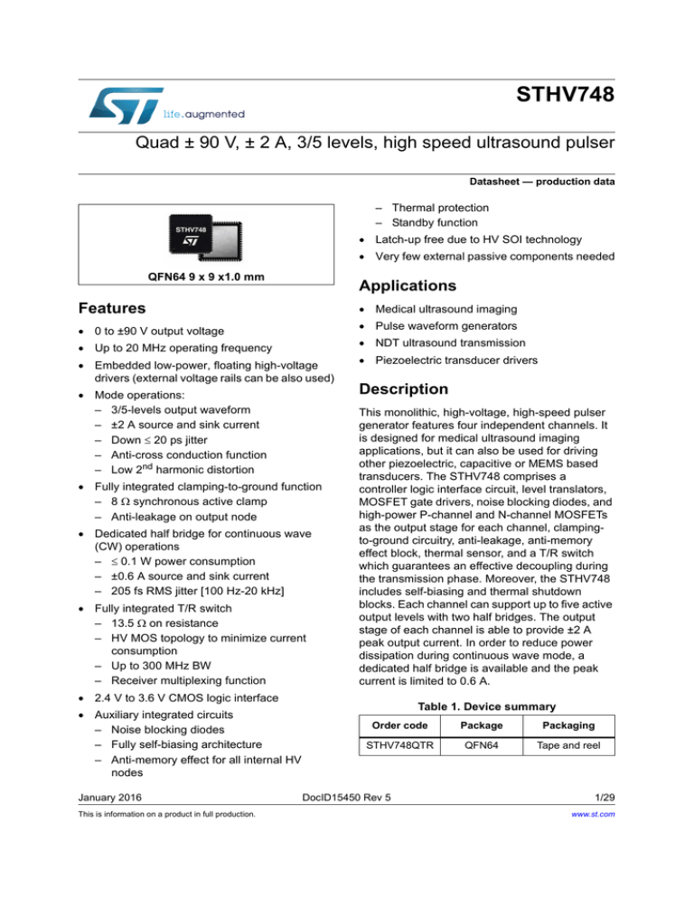
STHV748
Quad ± 90 V, ± 2 A, 3/5 levels, high speed ultrasound pulser
Datasheet — production data
– Thermal protection
– Standby function
Latch-up free due to HV SOI technology
Very few external passive components needed
QFN64 9 x 9 x1.0 mm
Applications
Features
Medical ultrasound imaging
0 to ±90 V output voltage
Pulse waveform generators
NDT ultrasound transmission
Up to 20 MHz operating frequency
Embedded low-power, floating high-voltage
drivers (external voltage rails can be also used)
Mode operations:
– 3/5-levels output waveform
– ±2 A source and sink current
– Down 20 ps jitter
– Anti-cross conduction function
– Low 2nd harmonic distortion
Fully integrated clamping-to-ground function
– 8 synchronous active clamp
– Anti-leakage on output node
Dedicated half bridge for continuous wave
(CW) operations
– 0.1 W power consumption
– ±0.6 A source and sink current
– 205 fs RMS jitter [100 Hz-20 kHz]
Fully integrated T/R switch
– 13.5 on resistance
– HV MOS topology to minimize current
consumption
– Up to 300 MHz BW
– Receiver multiplexing function
Piezoelectric transducer drivers
Description
This monolithic, high-voltage, high-speed pulser
generator features four independent channels. It
is designed for medical ultrasound imaging
applications, but it can also be used for driving
other piezoelectric, capacitive or MEMS based
transducers. The STHV748 comprises a
controller logic interface circuit, level translators,
MOSFET gate drivers, noise blocking diodes, and
high-power P-channel and N-channel MOSFETs
as the output stage for each channel, clampingto-ground circuitry, anti-leakage, anti-memory
effect block, thermal sensor, and a T/R switch
which guarantees an effective decoupling during
the transmission phase. Moreover, the STHV748
includes self-biasing and thermal shutdown
blocks. Each channel can support up to five active
output levels with two half bridges. The output
stage of each channel is able to provide ±2 A
peak output current. In order to reduce power
dissipation during continuous wave mode, a
dedicated half bridge is available and the peak
current is limited to 0.6 A.
2.4 V to 3.6 V CMOS logic interface
Auxiliary integrated circuits
– Noise blocking diodes
– Fully self-biasing architecture
– Anti-memory effect for all internal HV
nodes
January 2016
This is information on a product in full production.
Table 1. Device summary
Order code
Package
Packaging
STHV748QTR
QFN64
Tape and reel
DocID15450 Rev 5
1/29
www.st.com
Contents
STHV748
Contents
1
Typical application circuit . . . . . . . . . . . . . . . . . . . . . . . . . . . . . . . . . . . . 3
2
Pin settings . . . . . . . . . . . . . . . . . . . . . . . . . . . . . . . . . . . . . . . . . . . . . . . . 4
2.1
Connection . . . . . . . . . . . . . . . . . . . . . . . . . . . . . . . . . . . . . . . . . . . . . . . . . 4
2.2
Description . . . . . . . . . . . . . . . . . . . . . . . . . . . . . . . . . . . . . . . . . . . . . . . . . 4
2.3
Additional pin description . . . . . . . . . . . . . . . . . . . . . . . . . . . . . . . . . . . . . . 6
3
Truth table and single channel block description . . . . . . . . . . . . . . . . . 8
4
Power-up / Power-down voltage sequence . . . . . . . . . . . . . . . . . . . . . . 9
5
Electrical data . . . . . . . . . . . . . . . . . . . . . . . . . . . . . . . . . . . . . . . . . . . . . 10
5.1
6
Absolute maximum ratings . . . . . . . . . . . . . . . . . . . . . . . . . . . . . . . . . . . . 10
Operating supply voltages and average currents . . . . . . . . . . . . . . . . 11
6.1
Digital inputs . . . . . . . . . . . . . . . . . . . . . . . . . . . . . . . . . . . . . . . . . . . . . . . .11
6.2
Output signals . . . . . . . . . . . . . . . . . . . . . . . . . . . . . . . . . . . . . . . . . . . . . 12
7
Electrical characteristics . . . . . . . . . . . . . . . . . . . . . . . . . . . . . . . . . . . . 13
8
Timings . . . . . . . . . . . . . . . . . . . . . . . . . . . . . . . . . . . . . . . . . . . . . . . . . . . 16
9
Oscilloscope acquisitions . . . . . . . . . . . . . . . . . . . . . . . . . . . . . . . . . . . 21
9.1
Output phase noise measurement in CW mode . . . . . . . . . . . . . . . . . . . 24
9.1.1
10
Package information . . . . . . . . . . . . . . . . . . . . . . . . . . . . . . . . . . . . . . . . 25
10.1
11
2/29
Typical performance characteristics . . . . . . . . . . . . . . . . . . . . . . . . . . . 24
QFN64 9 x 9 x 1.0 mm 64 pitch 0.50 package information . . . . . . . . . . . 25
Revision history . . . . . . . . . . . . . . . . . . . . . . . . . . . . . . . . . . . . . . . . . . . 28
DocID15450 Rev 5
DocID15450 Rev 5
'B&75
'*1'
9WR9
GLJLWDOLQSXWV
,1
,1
,1
,1
'9''
9
ORJLF
1BGUY
3BGUY
+90
&:
+93
WR9
9
9''0
1BGUY
3BGUY
9''3
9
$*1'
7;
WR9
+90
1BGUY
3BGUY
7;
+93
WR9
*1'B3:5
DQWL
PHPRU\
+909
+909
+939
+939
,17B%,$6
9
+956:
&Q Q)
/9287
5()B+90
&Q Q)
67+9
7KHUPDO3URWHFWLRQ
;'&5
7+6'
+9287
5()B+93
6HOI9ROWDJH5HIHUHQFH
5()B+90
&K'
&K&
&K%
&K$
5()B+93
&S Q)
&S Q)
/1$
;
9
1
DQWLOHDNDJH
WR9
STHV748
Typical application circuit
Typical application circuit
Figure 1. Typical application circuit
53 .ё
$09
3/29
29
FODPS
Pin settings
STHV748
2
Pin settings
2.1
Connection
'9''
,1B'
,1B'
9''3
,1B'
*1'B3:5
/9287B'
;'&5B'
;'&5B$
,1B$
/9287B$
,1B$
9''0
,1B$
*1'B3:5
,17B%,$6
Figure 2. Pin connection (top view)
'*1'
$*1' 5()B+90 5()B+90
+90B$ +90B'
67+9
+90B$ +90B'
+9287B$ +9287B'
+93B'
+93B$ 5()B+93
5()B+93 +93B$ +93B'
+93B% +93B&
5()B+93
5()B+93 +93B&
+93B% +9287B% +9287B&
+90B% +90B&
+90B% +90B&
5()B+90
5()B+90 $*1'
,1B&
,1B&
,1B&
7+6'
9''0
*1'B3:5
*1'B3:5
9''3
;'&5B&
/9287B&
;'&5B%
/9287B%
,1B%
,1
,1B%
,1B%
'B&75 +99
2.2
Description
Table 2. Pin description (P = power, A = analog, D = digital)
4/29
Pin N
Name
1
AGND
2
REF_HVM1
3
Function
IN/OUT
Type
Signal ground
I
A
Supply for low side 1 gate driver
I
P
HVM1_A
Negative high-voltage supply 1 channel A
I
P
4
HVM0_A
Negative high-voltage supply 0 channel A
I
P
5
HVOUT_A
Channel A, high-voltage output before noise blocking
diodes
O
P
6
HVP0_A
Positive high-voltage supply 0 channel A
I
P
7
REF_HVP1
Supply for high side 1 gate driver
I
P
8
HVP1_A
Positive high-voltage supply 1 channel A
I
P
9
HVP1_B
Positive high-voltage supply 1 channel B
I
P
10
REF_HVP0
Supply for high side 0 gate driver
I
P
11
HVP0_B
Positive high-voltage supply 0 channel B
I
P
DocID15450 Rev 5
STHV748
Pin settings
Table 2. Pin description (P = power, A = analog, D = digital) (continued)
Pin N
Name
12
HVOUT_B
13
Function
IN/OUT
Type
Channel B, high-voltage output before noise blocking
diodes
O
P
HVM0_B
Negative high-voltage supply 0 channel B
I
P
14
HVM1_B
Negative high-voltage supply 1 channel B
I
P
15
REF_HVM0
Supply for low side 0 gate driver
I
P
16
D_CTR
Delay control
I
A
17
IN4
Input signal shared
I
D
18
IN1_B
Input signal channel B
I
D
19
IN2_B
Input signal channel B
I
D
20
IN3_B
Input signal channel B
I
D
21
VDDP
Positive low-voltage supply
I
A
22
GND_PWR
Power ground
I
P
23
XDCR_B
Channel B, high-voltage output
O
P
24
LVOUT_B
Channel B, low-voltage output
O
A
25
LVOUT_C
Channel C, low-voltage output
O
A
26
XDCR_C
Channel C, high-voltage output
O
P
27
GND_PWR
Power ground
I
P
28
VDDM
Negative low-voltage supply
I
A
29
IN3_C
Input signal channel C
I
D
30
IN2_C
Input signal channel C
I
D
31
IN1_C
Input signal channel C
I
D
32
THSD
Thermal shutdown pin
I/O
D
33
AGND
Signal ground
I
A
34
REF_HVM1
Supply for low side 1 gate driver
I
P
35
HVM1_C
Negative high-voltage supply 1 channel C
I
P
36
HVM0_C
Negative high-voltage supply 0 channel C
I
P
37
HVOUT_C
Channel C, high-voltage output before noise blocking
diodes
O
P
38
HVP0_C
Positive high-voltage supply 0 channel C
I
P
39
REF_HVP1
Supply for high side 1 gate driver
I
P
40
HVP1_C
Positive high-voltage supply 1 channel C
I
P
41
HVP1_D
Positive high-voltage supply 1 channel D
I
P
42
REF_HVP0
Supply for high side 0 gate driver
I
P
43
HVP0_D
Positive high-voltage supply 0 channel D
I
P
44
HVOUT_D
Channel D, high-voltage output before noise blocking
diodes
O
P
DocID15450 Rev 5
5/29
29
Pin settings
STHV748
Table 2. Pin description (P = power, A = analog, D = digital) (continued)
Pin N
Name
45
HVM0_D
46
HVM1_D
47
REF_HVM0
48
IN/OUT
Type
Negative high-voltage supply 0 channel D
I
P
Negative high-voltage supply 1 channel D
I
P
Supply for low side 0 gate driver
I
P
DGND
Logic ground
I
A
49
DVDD
Positive logic supply
I
A
50
IN1_D
Input signal channel D
I
D
51
IN2_D
Input signal channel D
I
D
52
IN3_D
Input signal channel D
I
D
53
VDDP
Positive low-voltage supply
I
A
54
GND_PWR
Power ground
I
P
55
XDCR_D
Channel D, high-voltage output
O
P
56
LVOUT_D
Channel D, low-voltage output
O
A
57
LVOUT_A
Channel A, low-voltage output
O
A
58
XDCR_A
Channel A, high-voltage output
O
P
59
GND_PWR
Power ground
I
P
60
VDDM
Negative low-voltage supply
I
A
61
IN3_A
Input signal channel A
I
D
62
IN2_A
Input signal channel A
I
D
63
IN1_A
Input signal channel A
I
D
64
INT_BIAS
Enable internal supply generators
I
D
Substrate
I
P
Exposed-Pad
2.3
Function
Additional pin description
The INT_BIAS pin enables the internal reference generators. With INT_BIAS=DVDD, the
STHV748 internally generates the reference voltages on REF_HVP1/0 (pin - 7, 10, 39, 42)
and REF_HVM1/0 (pin - 2, 15, 34, 47). These voltages are set at VDDP below HVP and
respectively at:
REF_HVM# = HVM# + VDDP
REF_HVP# = HVP# - VDDP
After enabling INT_BIAS, a period of time is needed to charge the external reference
capacitors (about 30 µs in a typical application).
Should INT_BIAS=DGND, it is necessary to apply an external voltage reference to the
REF_HVM# and REF_HVP# pins.
THSD is a thermal flag. Being the output stage of the THSD a Nch-MOS open-drain, an
external pull-up resist or (Rp10 k) connected to a positive low-voltage supply (see
Figure 1) is required. If the internal temperature surpasses 153 °C, THSD goes down and all
STHV748 channels are in HZ state. The thermal protection can be disabled, by connecting
6/29
DocID15450 Rev 5
STHV748
Pin settings
the THSD pin to a positive low voltage supply. THSD can be also shared among several
STHV748 on the same PCB.
D_CTR can be used to optimize 2nd HD performances by tuning the fall propagation delay
(tdf - see Table 9). If D_CTR is equal to ground, tdf has the nominal value. If D_CTR is
varied from 2 V to 4.2 V, tdf can be changed from -1 ns to +600 ps with respect to the
nominal value.
The exposed-pad is internally connected to the substrate of the package. It can be either left
floating or connected to a ground via 100 V capacitance toward ground, in order to reduce
the noise during the receiving phase.
5()B+90
/1$
&Q
67+9
7KHUPDO3URWHFWLRQ
9H[WHUQDOYROWDJHUHIHUHQFH
WR9
9H[WHUQDOYROWDJHUHIHUHQFH
+90
1BGUY
3BGUY
&Q
5()B+90
*1'B3:5
+956:
DQWL
PHPRU\
+909
+909
+939
+939
7;
+93
WR9
FODPS
9''0
1BGUY
WR9
9
+90
1BGUY
3BGUY
&:
3BGUY
9''3
9
+93
7;
$*1'
DQWLOHDNDJH
'*1'
'B&75
9WR9
GLJLWDOLQSXWV
,1
,1
,1
,1
'9''
9
ORJLF
WR9
/9287
;'&5
7+6'
6HOI9ROWDJH5HIHUHQFH
&K'
&K&
&K%
&K$
,17B%,$6
&S
5()B+93
&S
9H[WHUQDOYROWDJHUHIHUHQFH
9H[WHUQDOYROWDJHUHIHUHQFH
5()B+93
+9287
9
;
53
Figure 3. Typical application with INT_BIAS shorted to ground
$09
DocID15450 Rev 5
7/29
29
Truth table and single channel block description
3
STHV748
Truth table and single channel block description
3
3
,1
,1
7+6'
/HYHOVKLIWHUJDWHGULYHU
,1
,1
+9 3
+93 Figure 4. Single channel block description
3
6
1
3&:
6
3
6
7KHUPDO
KHUPDO
VHQVRUB
HQVRUB
7KHUPDO
HUPDO
QVRUB
VHQVRUB
1
+9 287
3&:
1&:
&/$03
1
1
1&:
6
6
756:
1RL VH
EOR FNLQ J
GLRG HV
&/$03
&/$
/ 03
6
6
75B6,*1$/
7;
75B6,*1$/
&O DPS
&:
6
*1'B3:5
+90 7;
+90 7RWKHUPDOSURWHFWLRQ
; '& 5
6
756:
756:
/9 287
6
*1'B3 :5
75 VZLWFK
$0Y
Table 3. Truth table for one channel
Global
Switches internal state
Per channel
State
THSD IN4 IN3 IN2 IN1
8/29
S0 S1 S2 S3 S4 S5 S6 S7 S8 S9
1
x
x
0
0
Clamp
0
0
0
0
0
0
1
0
1
0
1
0
0
0
1
HVM0
0
1
0
0
0
0
0
0
1
0
1
0
0
1
0
HVP0
1
0
0
0
0
0
0
0
1
0
1
x
0
1
1
T/R SW
0
0
0
0
0
0
1
1
0
1
1
0
1
0
1
HVM1
0
0
0
1
0
0
0
0
1
0
1
0
1
1
0
HVP1
0
0
1
0
0
0
0
0
1
0
1
0
1
1
1
HZ
0
0
0
0
0
0
0
0
1
0
1
1
1
1
1
T/R SW
0
0
0
0
0
0
1
1
0
1
1
1
0
0
1
Max. HVM0 and HVM1
0
1
0
1
0
0
0
0
1
0
1
1
0
1
0
Max. HVP0 and HVP1
1
0
1
0
0
0
0
0
1
0
1
1
1
0
1
CW HVM1
0
0
0
0
0
1
0
0
1
0
1
1
1
1
0
CW HVP1
0
0
0
0
1
0
0
0
1
0
0
x
x
x
x
HZ
0
0
0
0
0
0
0
0
1
0
DocID15450 Rev 5
STHV748
4
Power-up / Power-down voltage sequence
Power-up / Power-down voltage sequence
During the power up/power down phases, the following relationship must be always
respected:
VDDP >= DVDD
HVM0 <= HVM1
HVP0 >= HVP1
It is recommended to power up the low voltage supplies before the high voltage supplies.
DocID15450 Rev 5
9/29
29
Electrical data
STHV748
5
Electrical data
5.1
Absolute maximum ratings
Table 4. Absolute maximum ratings
Symbol
Parameter
Value
Unit
0
V
AGND
Analog ground reference (1)
DGND
Digital ground
-300 to 300
mV
GND_PWR
Power ground
-1.2 to 1.2
V
VDDP
Positive supply voltage
-0.3 to 3.9
V
VDDM
Negative supply voltage
0.3 to -3.9
V
DVDD
Positive logic voltage
-0.3 to VDDP
V
HVP0
TX0 high-voltage positive supply
95
V
HVP1
TX1 high-voltage positive supply
0 to HVP0
V
HVM0
TX0 high-voltage negative supply
-95
V
HVM1
TX1 high-voltage negative supply
0 to HVM0
V
REF_HVP#
High-voltage positive gate supply
-0.3 < HVP - REF_HVP < 3.6
V
REF_HVM#
High-voltage negative gate supply
-0.3 < REF_HVM - HVM < 3.6
V
High-voltage output
-95 to 95
V
HVOUT
High-voltage output before noise blocking diodes
-95 to 95
V
LVOUT
Low-voltage output
-1 to 1
V
DIG I/O
Digital input specified in Table 2
-0.3 to DVDD + 0.3
V
D_CTR
Delay control
-0.3 to 4.6
V
Operating temperature range
-40 to 125
°C
Storage temperature range
-65 to 150
°C
XDCR
TOP
TSTG
1. AGND is the ground reference for all the other voltages.
Note:
Absolute maximum ratings are those values beyond which damage to the device may occur.
Functional operation under these conditions is not implied.
Table 5. Thermal data
Symbol
Parameter
Value
Unit
Rth,JA
Thermal resistance junction-ambient
30 (1)
°C/W
1. This value is given for a two layer PCB (2S2P) and it’s strongly sensitive to PCB layout. Increasing the
number of PCB layers and/or adding heat sinks vias, the thermal resistance value decreases.
10/29
DocID15450 Rev 5
STHV748
6
Operating supply voltages and average currents
Operating supply voltages and average currents
Operating conditions, unless otherwise specified, only ONE channel on, no load, HV=90 V,
TX0 and TX1 on, INT_BIAS=DVDD, DVDD=3 V, VDDP=3 V and VDDM=-3 V
Table 6. Supply voltages and average currents
Symbol
VDDP
IVDDP
Parameter
Conditions
IVDDM
I_DVD
Standby mode
IHVP
IHVM
2.7
3
3.6
V
1.5
mA
1.1
-2.7
PW mode
-3
mA
-3.6
-1.5
V
mA
Negative supply current
Standby mode
-800
µA
min(3.6,V
DDP+0.3)
V
PW mode
100
µA
Standby mode
85
µA
90
V
1
mA
350
µA
0
V
Positive logic voltage
2.4
3
Logic supply current
High-voltage positive supply
0
PW mode
HV positive supply current
IHVP_Q
HVM
Units
(2)
Negative supply voltage
I_DVD_Q
HVP
Max.
PW mode (1)
Positive supply current
IVDDM_Q
DVDD
Typ.
Positive supply voltage
IVDDP_Q
VDDM
Min.
Standby mode
High-voltage negative supply
-90
PW mode
-1
mA
-350
µA
HV negative supply current
IHVM_Q
Standby mode
HVP-REF_HVP High-voltage positive gate supply
2.7
3
3.6
V
REF_HVM-HVM High-voltage negative gate supply
2.7
3
3.6
V
4.2
V
Max.
Units
DVDD
V
0.2 DVDD
V
D_CTR
Delay control
0
1. In PW pulse wave mode the average current is measured over T_w time (see Figure 6).
2. In standby mode all channels are in HZ and INT_BIAS= AGND
6.1
Digital inputs
Table 7. Digital inputs
Symbol
Parameter
Min.
IN1_#, IN2_#, IN3_#, IN4, INT_BIAS,
THSD
Input logic high-voltage 0.8 DVDD
IN1_#, IN2_#, IN3_#, IN4, INT_BIAS,
THSD
Input logic low-voltage
DocID15450 Rev 5
0
11/29
29
Operating supply voltages and average currents
6.2
STHV748
Output signals
Table 8. Output signals
Symbol
Parameter
Min.
Max.
Units
-90
90
V
High-voltage output
-90
90
V
LVOUT Low-voltage output
-1
1
V
THSD
0
3
V
HVOUT High-voltage output before noise blocking diodes
XDCR
12/29
Thermal shutdown pin
DocID15450 Rev 5
STHV748
7
Electrical characteristics
Electrical characteristics
Table 9. Static electrical characteristics (1)
Symbol
Parameter
Condition
Min.
Typ.
1.1
1.30
A
HVP# =25 V, HVM# =-25 V,
HVOUT=0 V
1.70
A
HVP# =90 V, HVM# =-90 V,
HVOUT=0 V
2
A
1.30
A
HVP# =25 V, HVM# =-25 V,
HVOUT=0 V
1.70
A
HVP# =90 V, HVM# =-90 V,
HVOUT=0 V
2
A
HVP# =10 V, HVM# =-10 V,
HVOUT=0 V
IN
Saturation current S1 - S3
HVP# =10 V, HVM# =-10 V,
HVOUT=0 V
IP
Saturation current S0 - S2
1
Max.
Units
INCW
Saturation current S5
HVP1=10 V, HVM1=-10 V,
HVOUT=0 V
300
350
mA
IPCW
Saturation current S4
HVP1=10 V, HVM1=-10 V,
HVOUT=0 V
390
480
mA
ICL
Saturation current S6
HVOUT=25 V
1.5
A
HVOUT=1 V
8
W
HVP# = 90 V, HVM# = -90 V,
HVOUT=0 V
1
HVP# = 90 V, HVM# = -90 V,
HVOUT=-90 V
1
HVP# = 90 V, HVM# = -90 V,
HVOUT=+90 V
1
RON_CLAMP On resistance S6
IL
PSB
Output leakage current, per
channel
HVP# = 90 V, HVM# = -90 V,
Power dissipation in standby HVOUT=0 V, INT_BIAS=DGND
mode
HVP# = 90 V, HVM# = -90 V,
HVOUT=0 V
µA
4
126
µW
150
mW
P
RX
Power dissipation in
HVR_SW state
HVP# = 30 V, HVM# = -30 V,
INT_BIAS =0, all channels in
receiving phase
V
REFP
HVP# - REF_HVP#
HVP# = 10 V, HVM# = -10 V,
HVOUT=0 V
0.8
VDDP
1.2
VDDP
V
VREFN
REF_HVM# - HVM#
HVP# = 10 V, HVM# = -10 V,
HVOUT=0 V
0.8
VDDP
1.2
VDDP
V
TOTP(2)
Overtemperature threshold
HVP# =10 V, HVM# =-10 V
160
°C
OTP hysteresis
HVP# =10 V, HVM# =-10 V
T
HYS
DocID15450 Rev 5
30
130
153
40
mW
°C
13/29
29
Electrical characteristics
STHV748
Table 9. Static electrical characteristics (1) (continued)
Symbol
Parameter
CT/R SW
T/R SW capacitance
LVOUT=0 V
T/R SW on resistance
HVP# =10 V, HVM# =-10 V,
XDCR=0 V, LVOUT=0.2 V
T/R SW off resistance
HVP# =10 V, HVM# =-10 V,
XDCR=1 V, LVOUT=0 V
R
T/R SW_ON
R
T/R
SW_OFF
Condition
Min.
Typ.
Max.
40
Voltage drop between HVP1 HVP# =10V, HVM# =-10V,
ISINK_XDCR=50 mA
VDROP_C and XDCR
W
Voltage drop between XDCR HVP# =10V, HVM# =-10V,
and HVM1
ISOURCE_XDCR=50 mA
Units
pF
13.5
15.5
1
W
G
2.58
2.79
2.9
V
2.58
2.86
2.9
V
1. Operating conditions, unless otherwise specified, INT_BIAS=DVDD, HVP# = 90 V, HVM# = -90 V, VDDP = 3 V, VDDM = 3 V, DVDD = 3 V, TROOM = 25 °C.
2. Guaranteed by bench characterization.
Table 10. AC electrical characteristics (1)
Symbol
Parameter
Test condition
Min. Typ. Max.
16
f
MHz
50 pF//200
22
MHz
fCW
Maximum output frequency CW
HVP1 =5 V, HVM1 = -5 V,
continuous wave mode
20
MHz
fBW
Output frequency BW
HVP1 = 50 V, HVM1 = -50 V,
continuous wave mode, 50
pF//200
10
MHz
tj-CW
CW output jitter
HVP1 =5 V, HVM1 = -5 V,
continuous wave mode
205
fs, rms
tf
Fall time
28
ns
tr
Rise time
28
ns
tdr
Rise propagation delay
24
ns
tdf
Fall propagation delay
24
ns
T/R SW turn-on / turn-off time
170
ns
1 pulse f = 1.7 MHz
-40
dBc
1 pulse f = 5 MHz
-40
dBc
5 pulses f = 1.7 MHz
-40
dBc
5 pulses f = 5 MHz
-40
dBc
f = 1.7 MHz original and
inverted pulse
-40
dBc
f = 5 MHz original and
inverted pulse
-40
dBc
2
%
T/R SW
HD2
HD2PC
BVD
14/29
Maximum output frequency
Units
2nd harmonic distortion
Pulse cancellation
Burst voltage drop
1st to 128th pulse HVP1 = 10
V, HVM1 = -10 V
DocID15450 Rev 5
STHV748
Electrical characteristics
Table 10. AC electrical characteristics (1)
Symbol
Parameter
Test condition
Min. Typ. Max.
Power dissipation, all channels
CW mode, f = 5 MHz, HVP1 =
5 V, HVM1 = -5 V, no load
390
Power dissipation, one channel
CW mode, f = 5 MHz, HVP1 =
5 V, HVM1 = -5 V
PD_CW
T/R SWSPIKE
XTALK
Units
mW
T/R SW spike on XDCR and LVOUT
Cross talk between channels.
Ampl(2ch)/Ampl(1ch), 50
pF//200
320
100
mVpp
-40
db
1. Operating conditions, unless otherwise specified, HVP# = 90 V, HVM# = -90 V, VDDP = 3 V, VDDM = -3 V, DVDD = 3 V,
V, INT_BIAS = DVDD, (HVP-REF_HVP) = 3 V, (REF_HVM-HVM) = 3 V, XDCR load C = 300 pF//R = 100 , LVOUT load C
= 20 pF//200 TROOM = 25 °C.
DocID15450 Rev 5
15/29
29
Timings
8
STHV748
Timings
Figure 5. tr, tf, tdr, and tdf descriptions
,1
,1
,1
7GI 7 I
,1
7 GU 7 U
+93
+93
;'&5
+93
;'&5
+90
+90
+90
$0Y
Figure 6. PW example 5 periods, HVP0 = 90 V, HVM0 = -90 V, T=200 ns, T_tx=1.2 µs,
T_w=200 µs
,1
,1
,1
,1
+93
;'&5
+90
WKSHULRG
7
FODPS
7BK
7BW[ WUDQVPLVVLRQSHULRG
7BZ (QWLUHZDIHIRUP
$0Y
16/29
DocID15450 Rev 5
STHV748
Timings
Figure 7. PW and HD2 example (HVP0=80 V, HVM0=-80 V load 300 pF//100 )
Figure 8. PC example, HVP0 = 90 V HVM0 = -90 V, T=200 ns, T_pos= T_neg=400 ns
,1
,1
,1
,1
+93
7
;'&5
;'&5B 3&
7BSRV
+90
7BQHJ
7BQHJ
))7ZLQGRZ
$0Y
DocID15450 Rev 5
17/29
29
Timings
STHV748
Figure 9. CW mode example, HVP1 = 5 V, HVM1 = 5 V, T = 200 ns, T_tx>1 ms
,1
,1
,1
,1
7
7BW[
7BK
$0Y
Figure 10. T/R SW signal equivalent circuit model
XDCR
LVOUT
Rs/2
Rs/2
Rp
Cp
Rs=13 Ω
Rp=100 KΩ
Cp=40 pF
AGND
AM020067v1
18/29
DocID15450 Rev 5
STHV748
Timings
Figure 11. T/R SW bandwidth
DocID15450 Rev 5
19/29
29
Timings
STHV748
Figure 12. Possible external connection for LVOUT outputs with T/R SW in multiplexing driving
configuration
Ć
67+9
&+B$
6LQJOHĆ5;ĆFKDLQĆ
;'&5B$
+95B6:
7;
08;ĆFRPPDQGĆ W
&+B%
/1$
7*&
3*$
(&+2Ć6,*1$/W
/3
)LOWHU
$'&
$)(
/9287B$
;'&5B%
+95B6:
7;
08;ĆFRPPDQGĆ WẄ (&+2Ć6,*1$/WẄ /9287B%
&+B&
;'&5B&
+95B6:
7;
08;ĆFRPPDQGĆ W¨W &+B'
(&+2Ć6,*1$/WẄ /9287B&
;'&5B'
08;ĆFRPPDQGĆ W¨W +95B6:
7;
(&+2Ć6,*1$/WẄ /9287B'
$0Y
20/29
DocID15450 Rev 5
STHV748
9
Oscilloscope acquisitions
Oscilloscope acquisitions
Figure 13. TX0 = ±60 V positive-negative pulses and immediately after TX1 = ±30 V
positive-negative pulses, load 300 pF // 100
Figure 14. Five-levels HV output voltage
DocID15450 Rev 5
21/29
29
Oscilloscope acquisitions
STHV748
Figure 15. CW operations at 6 MHz
Figure 16. CW operations at 9 MHz
22/29
DocID15450 Rev 5
STHV748
Oscilloscope acquisitions
Figure 17. Two positive and two negative “short pulses” with 10 ns time width for
inputs IN#, HVP/N/0/1 = ±90 V, load 300 pF // 100 .
DocID15450 Rev 5
23/29
29
Oscilloscope acquisitions
STHV748
9.1
Output phase noise measurement in CW mode
9.1.1
Typical performance characteristics
Unless otherwise stated, the following conditions apply:
VDDP = +3.3 V, VDDM = -3.3 V, DVDD = +3.3 V, Exp-PAD = -5 V, HVP = +5 V, HVM = -5 V,
no load, Fin= 5 MHz, TA = 25 °C.
Figure 18. Measurement setup - CK1 = 640 MHz; CK2 = 5 MHz
Figure 19. Phase noise output plot
56)6836LJQDO6RXUFH$QDO\]HU
6HWWLQJV
6LJQDO)UHTXHQF\
0+]
,QW3+1NG%F
6LJQDO/HYHO
G%P
5HVLGXDO30
3//0RGH
+DUPRQLF
5HVLGXDO)0
+]
,QWHUQDO5HI7XQHG ,QWHUQDO3KDVH'HW506-LWWHU
3KDVH1RLVH>G%F+]@
5)$WWHQ
G%
7RSG%F+]
/2&.('
5HVLGXDO1RLVH>7ZRVSXUV@
3KDVH'HWHFWRUG%
SV
0DUNHU>7@
N+]
G%F+]
6
P6
$
6*/
&/5:5
607+
&/5:5
(/ (/
6352))
7+G%
/RRS%:+]
+]
N+]
)UHTXHQF\2IIVHW
N+]
N+]
Significant results from the output have been extracted(a):
–
Phase noise @1 kHz: -147 dBc/Hz
–
RMS jitter [BW 100 Hz - 20 KHz]: 205 fs
a. Values measured leave room for improvement. As such, they are affected by a non-optimized setup.
24/29
DocID15450 Rev 5
STHV748
10
Package information
Package information
In order to meet environmental requirements, ST offers these devices in different grades of
ECOPACK® packages, depending on their level of environmental compliance. ECOPACK
specifications, grade definitions and product status are available at: www.st.com.
ECOPACK is an ST trademark.
10.1
QFN64 9 x 9 x 1.0 mm 64 pitch 0.50 package information
Figure 20. QFN64 9 x 9 x 1.0 mm 64 pitch 0.50 package outline
3FW#
DocID15450 Rev 5
25/29
29
Package information
STHV748
Table 11. QFN64 9 x 9 x 1.0 mm 64 pitch 0.50 package mechanical data
Dim
Min.
Typ.
Max.
A
0.8
0.9
1
A1
0.02
0.05
A2
0.65
1
A3
0.2
b
0.18
0.25
0.3
D
8.85
9
9.15
D1
8.75
D2
See exposed pad variation
E
8.85
9
E1
9.15
8.75
E2
See exposed pad variation
e
0.5
L
0.35
0.4
0.45
P
0.6
K
12
ddd
0.08
Table 12. Exposed-pad variation
6D2
E2
Variation
Note:
26/29
Min.
Typ.
Max.
Min.
Typ.
Max.
A
4.1
4.25
4.4
4.1
4.25
4.4
B
4.55
4.7
4.85
4.55
4.7
4.85
C
6.95
7.1
7.25
6.95
7.1
7.25
D
7.15
7.3
7.45
7.15
7.3
7.45
QFN64 used for STHV748 has D variation option.
DocID15450 Rev 5
STHV748
Package information
Figure 21. QFN64 9 x 9 x 1.0 mm 64 tape and reel information
mm.
inch
DIM.
MIN.
A
TYP .
MAX.
MIN.
330
MAX.
12.992
C
12.8
D
20.2
0.795
N
60
2.362
T
13.2
TYP.
0.504
30.4
0.519
1.196
Ao
12.25
12.45
0482
0.490
Bo
12.25
12.45
0482
0.490
Ko
2.1
2.3
0.083
0.091
Po
3.9
4.1
0.153
0.161
P
15.9
16.1
0.626
0.639
DocID15450 Rev 5
27/29
29
Revision history
11
STHV748
Revision history
Table 13. Document revision history
Date
Revision
20-Jan-2010
1
Initial release.
17-Feb-2010
2
Updated typo on coverpage.
3
Updated Table 6: Supply voltages and average currents,
Table 9: Static electrical characteristics and Table 10: AC
electrical characteristics.
Minor text changes.
4
Updated the entire Table 6: Supply voltages and average
currents title included.
Updated title in Figure 6: PW example 5 periods, HVP0 = 90 V,
HVM0 = -90 V, T=200 ns, T_tx=1.2 µs, T_w=200 µs.
Minor text changes.
5
– Updated Features on the coverpage and output jitter data in
Table 10.
– Added Section 9.1: Output phase noise measurement in CW
mode.
– Reformatted Package information section to current
standards.
– Minor text changes throughout the document.
09-Nov-2011
11-May-2012
20-Jan-2016
28/29
Changes
DocID15450 Rev 5
STHV748
IMPORTANT NOTICE – PLEASE READ CAREFULLY
STMicroelectronics NV and its subsidiaries (“ST”) reserve the right to make changes, corrections, enhancements, modifications, and
improvements to ST products and/or to this document at any time without notice. Purchasers should obtain the latest relevant information on
ST products before placing orders. ST products are sold pursuant to ST’s terms and conditions of sale in place at the time of order
acknowledgement.
Purchasers are solely responsible for the choice, selection, and use of ST products and ST assumes no liability for application assistance or
the design of Purchasers’ products.
No license, express or implied, to any intellectual property right is granted by ST herein.
Resale of ST products with provisions different from the information set forth herein shall void any warranty granted by ST for such product.
ST and the ST logo are trademarks of ST. All other product or service names are the property of their respective owners.
Information in this document supersedes and replaces information previously supplied in any prior versions of this document.
© 2016 STMicroelectronics – All rights reserved
DocID15450 Rev 5
29/29
29
