PRELIMINARY
CMPA1D1E030D
30 W, 13.75 - 14.5 GHz, 40 V, GaN MMIC, Power Amplifier
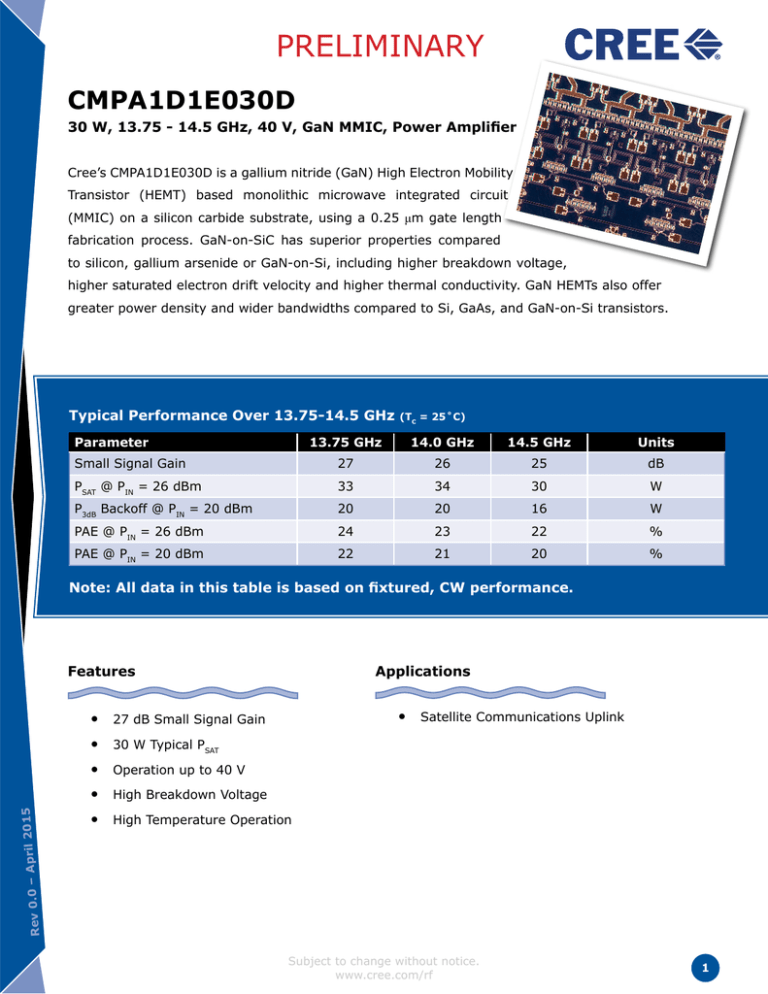
Cree’s CMPA1D1E030D is a gallium nitride (GaN) High Electron Mobility
Transistor (HEMT) based monolithic microwave integrated circuit
(MMIC) on a silicon carbide substrate, using a 0.25 μm gate length
fabrication process. GaN-on-SiC has superior properties compared
to silicon, gallium arsenide or GaN-on-Si, including higher breakdown voltage,
higher saturated electron drift velocity and higher thermal conductivity. GaN HEMTs also offer
greater power density and wider bandwidths compared to Si, GaAs, and GaN-on-Si transistors.
Typical Performance Over 13.75-14.5 GHz
Parameter
(TC = 25˚C)
13.75 GHz
14.0 GHz
14.5 GHz
Units
Small Signal Gain
27
26
25
dB
PSAT @ PIN = 26 dBm
33
34
30
W
P3dB Backoff @ PIN = 20 dBm
20
20
16
W
PAE @ PIN = 26 dBm
24
23
22
%
PAE @ PIN = 20 dBm
22
21
20
%
Note: All data in this table is based on fixtured, CW performance.
Features
Applications
• Satellite Communications Uplink
• 27 dB Small Signal Gain
• 30 W Typical PSAT
• Operation up to 40 V
il 2015
Rev 0.0 – Apr
• High Breakdown Voltage
• High Temperature Operation
Subject to change without notice.
www.cree.com/rf
1
Absolute Maximum Ratings (not simultaneous) at 25˚C
Symbol
Rating
Units
Conditions
Drain-source Voltage
Parameter
VDSS
84
VDC
25˚C
Gate-source Voltage
VGS
-10, +2
VDC
25˚C
Storage Temperature
TSTG
-55, +150
˚C
Operating Junction Temperature
TJ
225
˚C
Maximum Forward Gate Current
IGMAX
10
mA
25˚C
Maximum Drain Current1
IDMAX
0.6
A
Stage 1, 25˚C
Maximum Drain Current1
IDMAX
0.96
A
Stage 2, 25˚C
Maximum Drain Current
IDMAX
2.2
A
Stage 3, 25˚C
Thermal Resistance, Junction to Case2
RθJC
1.5
˚C/W
85˚C, PDISS = 94W
TS
320
˚C
30 seconds
1
Mounting Temperature (30 seconds)
Note Current limit for long term, reliable operation. Total current when biased from top and bottom drain pads.
Note2 Eutectic die attach using 80/20 AuSn mounted to a 20 mil thick CuMoCu carrier.
1
Electrical Characteristics (Frequency = 13.75 GHz to 14.5 GHz unless otherwise stated; TC = 25˚C)
Characteristics
Symbol
Min.
Typ.
Max.
Units
Conditions
VTH
-3.8
-2.8
-2.3
V
VDS = 10 V, ID = 18.2 mA
VBD
84
100
–
V
VGS = -8 V, ID = 18.2 mA
Small Signal Gain
S21
–
27
–
dB
VDD = 40 V, IDQ = 300 mA
Input Return Loss
S11
–
-16
–
dB
VDD = 40 V, IDQ = 300 mA
Output Return Loss
S22
–
-9
–
dB
VDD = 40 V, IDQ = 300 mA
Power Output
POUT1
–
50
–
W
VDD = 40 V, IDQ = 300 mA, CW, PIN = 24 dBm
Power Output
POUT2
–
24
–
W
VDD = 40 V, IDQ = 300 mA, PIN = 18 dBm
Power Added Efficiency
PAE1
–
30
–
%
VDD = 40 V, IDQ = 300 mA, CW, PIN = 24 dBm
Power Added Efficiency
PAE2
–
25
–
%
VDD = 40 V, IDQ = 300 mA, PIN = 18 dBm
GP
–
22
–
dB
VDD = 40 V, IDQ = 300 mA
VSWR
–
5:1
–
Y
No damage at all phase angles,
VDD = 40 V, IDQ = 300 mA, POUT = 25W CW
DC Characteristics
Gate Threshold
Drain-Source Breakdown Voltage
RF Characteristics
2
Power Gain
Output Mismatch Stress
Notes:
1
Scaled from PCM data.
2
All data pulse tested on-wafer with Pulse Width = 10 μs, Duty Cycle = 0.1%.
Copyright © 2014 Cree, Inc. All rights reserved. The information in this document is subject to change without notice. Cree and the
Cree logo are registered trademarks of Cree, Inc. Other trademarks, product and company names are the property of their respective
owners and do not imply specific product and/or vendor endorsement, sponsorship or association.
2
CMPA1D1E030D Rev 0, Preliminary
Cree, Inc.
4600 Silicon Drive
Durham, North Carolina, USA 27703
USA Tel: +1.919.313.5300
Fax: +1.919.869.2733
Fax: +1.919.869.2733
www.cree.com/RF
Block Diagram Showing Additional Capacitors for Operation Over 13.75 to 14.5 GHz
Designator
Description
Quantity
C1,C2,C3,C4,C5,C6,C7,C8,C9,C10
CAP, 51pF, +/-10%, SINGLE LAYER, 0.030”, Er 3300, 100V, Ni/
Au TERMINATION
10
C11,C12,C13,C14
CAP, 680pF, +/-10%, SINGLE LAYER, 0.070”, Er 3300, 100V,
Ni/Au TERMINATION
4
Notes:
1
The input, output and decoupling capacitors should be attached as close as possible to the
die- typical distance is 5 to 10 mils with a maximum of 15 mils.
2
The MMIC die and capacitors should be connected with 2 mil gold bond wires.
Copyright © 2014 Cree, Inc. All rights reserved. The information in this document is subject to change without notice. Cree and the
Cree logo are registered trademarks of Cree, Inc. Other trademarks, product and company names are the property of their respective
owners and do not imply specific product and/or vendor endorsement, sponsorship or association.
3
CMPA1D1E030D Rev 0, Preliminary
Cree, Inc.
4600 Silicon Drive
Durham, North Carolina, USA 27703
USA Tel: +1.919.313.5300
Fax: +1.919.869.2733
Fax: +1.919.869.2733
www.cree.com/RF
Die Dimensions (units in microns)
Overall die size 5000 x 6000 (+0/-50) microns, die thickness 100 (+/-10) microns.
All Gate and Drain pads must be wire bonded for electrical connection.
Pad Number
Function
Description
Pad Size (in)
Note
1
RF_IN
RF-Input pad. Matched to 50 ohm
102x252
5
2
VG1A bottom
Gate control for stage1. Vg = -2.0 to -3.5 V
128x125
1,2
3
VG1A top
Gate control for stage1. Vg = -2.0 to -3.5 V
128x125
1,2
4
VG2A bottom
Gate control for stage2. Vg = -2.0 to -3.5 V
128x125
1,2
5
VG2A top
Gate control for stage2. Vg = -2.0 to -3.5 V
128x125
1,2
6
VD1 bottom
Drain control for stage1. Vd = 40 V
128x125
1,3
7
VD1 top
Drain control for stage1. Vd = 40 V
128x125
1,3
8
VD2 bottom
Drain control for stage2. Vd = 40 V
128x125
1,4
9
VD2 top
Drain control for stage2. Vd = 40 V
128x125
1,4
10
VG3A bottom
Gate control for stage3. Vg = -2.0 to -3.5 V
128x125
1,2
11
VG3A top
Gate control for stage3. Vg = -2.0 to -3.5 V
128x125
1,2
12
VD3 bottom
Drain control for stage3. Vd = 40 V
328x125
1,4
13
VD3 top
Drain control for stage3. Vd = 40 V
328x125
1,4
14
RF_OUT
RF-Output pad. Matched to 50 ohm
102x302
5
Notes:
1
Attach bypass capacitor to pads 2-13 per aplications circuit
2
VG1A&2A&3A top and bottom are connected internally, so it would be enough to connect either one for proper operation
3
VD1 top and bottom are not connected internally and have to be biased from both sides for proper operation
4
For current handling, it is recommended to bias VD2 and VD3 from both top and bottom sides
5
The RF Input and Output pads have a ground-signal-ground with a nominal pitch of 10 mil (250 um). The RF ground pads are 102 x
102 microns
Die Assembly Notes:
•
Recommended solder is AuSn (80/20) solder. Refer to Cree’s website for the Eutectic Die Bond Procedure application note at
•
Vacuum collet is the preferred method of pick-up.
•
The backside of the die is the Source (ground) contact.
•
Die back side gold plating is 5 microns thick minimum.
•
Thermosonic ball or wedge bonding are the preferred connection methods.
•
Gold wire must be used for connections.
•
Use the die label (XX-YY) for correct orientation.
http://www.cree.com/~/media/Files/Cree/RF/Application%20Notes/Appnote%202%20Eutectic.pdf
Copyright © 2014 Cree, Inc. All rights reserved. The information in this document is subject to change without notice. Cree and the
Cree logo are registered trademarks of Cree, Inc. Other trademarks, product and company names are the property of their respective
owners and do not imply specific product and/or vendor endorsement, sponsorship or association.
4
CMPA1D1E030D Rev 0, Preliminary
Cree, Inc.
4600 Silicon Drive
Durham, North Carolina, USA 27703
USA Tel: +1.919.313.5300
Fax: +1.919.869.2733
Fax: +1.919.869.2733
www.cree.com/RF
Part Number System
CMPA1D1E030D
Package
Power Output (W)
Upper Frequency (GHz)
Lower Frequency (GHz)
Cree MMIC Power Amplifier Product Line
Parameter
Value
Units
Lower Frequency
13.75
GHz
Upper Frequency1
14.5
GHz
30
W
Bare Die
-
Power Output
Package
Table 1.
Note : Alpha characters used in frequency
1
code indicate a value greater than 9.9 GHz.
See Table 2 for value.
Character Code
Code Value
A
0
B
1
C
2
D
3
E
4
F
5
G
6
H
7
J
8
K
9
Examples:
1A = 10.0 GHz
2H = 27.0 GHz
Table 2.
Copyright © 2014 Cree, Inc. All rights reserved. The information in this document is subject to change without notice. Cree and the
Cree logo are registered trademarks of Cree, Inc. Other trademarks, product and company names are the property of their respective
owners and do not imply specific product and/or vendor endorsement, sponsorship or association.
5
CMPA1D1E030D Rev 0, Preliminary
Cree, Inc.
4600 Silicon Drive
Durham, North Carolina, USA 27703
USA Tel: +1.919.313.5300
Fax: +1.919.869.2733
Fax: +1.919.869.2733
www.cree.com/RF
Disclaimer
Specifications are subject to change without notice. Cree, Inc. believes the information contained within this data sheet
to be accurate and reliable. However, no responsibility is assumed by Cree for its use or for any infringement of patents
or other rights of third parties which may result from its use. No license is granted by implication or otherwise under
any patent or patent rights of Cree. Cree makes no warranty, representation or guarantee regarding the suitability of its
products for any particular purpose. “Typical” parameters are the average values expected by Cree in large quantities
and are provided for information purposes only. These values can and do vary in different applications, and actual
performance can vary over time. All operating parameters should be validated by customer’s technical experts for each
application. Cree products are not designed, intended, or authorized for use as components in applications intended for
surgical implant into the body or to support or sustain life, in applications in which the failure of the Cree product could
result in personal injury or death, or in applications for the planning, construction, maintenance or direct operation of a
nuclear facility. CREE and the CREE logo are registered trademarks of Cree, Inc.
For more information, please contact:
Cree, Inc.
4600 Silicon Drive
Durham, North Carolina, USA 27703
www.cree.com/RF
Sarah Miller
Marketing & Export
Cree, RF Components
1.919.407.5302
Ryan Baker
Marketing
Cree, RF Components
1.919.407.7816
Tom Dekker
Sales Director
Cree, RF Components
1.919.407.5639
Copyright © 2014 Cree, Inc. All rights reserved. The information in this document is subject to change without notice. Cree and the
Cree logo are registered trademarks of Cree, Inc. Other trademarks, product and company names are the property of their respective
owners and do not imply specific product and/or vendor endorsement, sponsorship or association.
6
CMPA1D1E030D Rev 0, Preliminary
Cree, Inc.
4600 Silicon Drive
Durham, North Carolina, USA 27703
USA Tel: +1.919.313.5300
Fax: +1.919.869.2733
Fax: +1.919.869.2733
www.cree.com/RF


