Preliminary Technical Data
Dual-Channel
Audio Difference Amplifier
AD8273
FEATURES
Two gain settings:
Gain of 1/2 (–6 dB)
Gain of 2 (6 dB)
0.03% max gain accuracy
10 ppm max gain drift
Excellent AC Specifications
25V/μs slew rate
0.9 μs to 0.01% settling time
Low Distortion
0.003% at 1 kHz
High Accuracy DC Performance
90 dB typ CMRR
250 uV max offset voltage
14 lead SOIC Package
Supply current: 2.5 mA per channel
Supply range: ±2.5 V to ±18 V
FUNCTIONAL BLOCK DIAGRAM
+VS
11
–IN1
2
12kΩ
SENSE1
13
OUT1
14
REF1
10
SENSE2
6kΩ
–
+
+IN1
–IN2
3
12kΩ
6kΩ
6
12kΩ
6kΩ
–
APPLICATIONS
High Performance Audio
Instrumentation Amplifier Building Block
Level Translator
Automatic Test Equipment
Sin/Cos Encoders
12
9
OUT2
+
+IN2
5
12kΩ
6kΩ
8
REF2
4
–VS
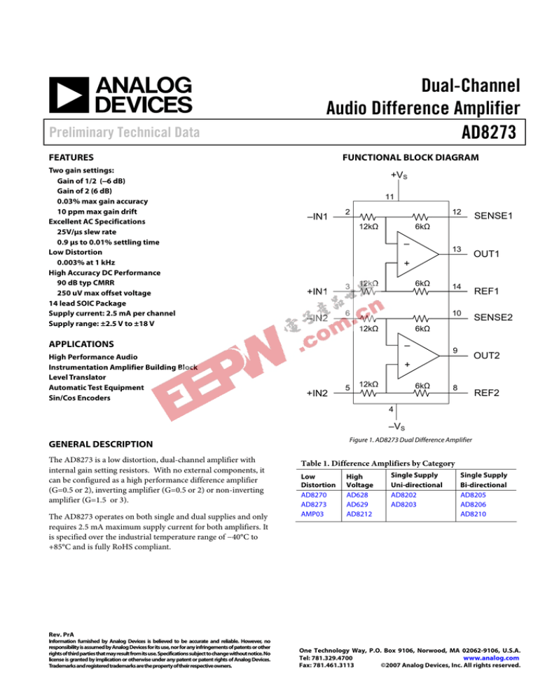
Figure 1. AD8273 Dual Difference Amplifier
GENERAL DESCRIPTION
The AD8273 is a low distortion, dual-channel amplifier with
internal gain setting resistors. With no external components, it
can be configured as a high performance difference amplifier
(G=0.5 or 2), inverting amplifier (G=0.5 or 2) or non-inverting
amplifier (G=1.5 or 3).
The AD8273 operates on both single and dual supplies and only
requires 2.5 mA maximum supply current for both amplifiers. It
is specified over the industrial temperature range of −40°C to
+85°C and is fully RoHS compliant.
Table 1. Difference Amplifiers by Category
Low
Distortion
AD8270
AD8273
AMP03
High
Voltage
AD628
AD629
AD8212
Single Supply
Uni-directional
AD8202
AD8203
Single Supply
Bi-directional
AD8205
AD8206
AD8210
Rev. PrA
Information furnished by Analog Devices is believed to be accurate and reliable. However, no
responsibility is assumed by Analog Devices for its use, nor for any infringements of patents or other
rights of third parties that may result from its use. Specifications subject to change without notice. No
license is granted by implication or otherwise under any patent or patent rights of Analog Devices.
Trademarks and registered trademarks are the property of their respective owners.
One Technology Way, P.O. Box 9106, Norwood, MA 02062-9106, U.S.A.
Tel: 781.329.4700
www.analog.com
Fax: 781.461.3113
©2007 Analog Devices, Inc. All rights reserved.
AD8273
Preliminary Technical Data
SPECIFICATIONS
VS = ±18 V, VREF = 0 V, TA = 25°C, G = 1/2, RL = 2 kΩ, unless otherwise noted.
Table 2.
Parameter
DYNAMIC PERFORMANCE
Bandwidth
Slew Rate
Settling Time to 0.1%
Settling Time to 0.01%
Channel Separation
NOISE/DISTORTION1
THD + Noise
Noise Floor, RTO
Output Voltage Noise (referred to input)
GAIN
Gain Error
Gain Drift
Gain Nonlinearity
INPUT CHARACTERISTICS
Offset3
vs. Temperature
vs. Power Supply
Common Mode Rejection Ratio
Conditions
Min
Typ
Max
Unit
10V Step on output, CL=100 pF
10V Step on output, CL=100 pF
f = 1 kHz
12
25
0.7
0.9
130
MHz
V/μs
μs
μs
dB
f = 1 kHz, VIN= 10 Vrms
20 kHz BW
f = 20 Hz to 20 kHz
f = 1 kHz
0.003
-120
3
20
%
dBu2
μVrms
nV/√Hz
1
10
VCM=±18V, RS=0Ω, referred to
input
Input Voltage Range
Impedance
Differential
Common Mode4
OUTPUT CHARACTERISTICS
Output Swing
Short circuit current limit
Capacitive Load Drive
POWER SUPPLY
Supply Current (per Amplifier)
TEMPERATURE RANGE
Specified Performance
77
200
2
5
86
-Vs-0.5
0.03
10
%
ppm/°C
ppm
400
μV
μV/°C
μV/V
dB
20
+VS+0.5
24
9
-Vs+1.5
kΩ
kΩ
+ VS -1.5
V
mA
pF
2.5
mA
60
100
-40
1
Includes amplifier voltage noise, resistor network voltage noise, and amplifier current noise through resistor network
dBu = 20log(Vrms/0.7746)
Includes effects of amplifier’s input bias and offset currents
4
Calculated looking into both inputs. Common mode impedance looking into only one input is 18 kΩ
2
3
Rev. PrA| Page 2 of 4
V
85
Preliminary Technical Data
AD8273
ABSOLUTE MAXIMUM RATINGS
Table 3.
Parameter
Supply Voltage
Output Short-Circuit Current
Input Voltage (Common Mode)
Differential Input Voltage
Storage Temperature Range
Specified Temperature Range
Thermal Resistance θJA
Thermal Resistance θJC
Package Glass Transition Temperature (TG)
Rating
TBD
Indefinite
TBD
TBD
−65°C to +130°C
−40°C to +85°C
120 °C/W
36 °C/W
130°C
Maximum Power Dissipation
The maximum safe power dissipation for the AD8273 is limited
by the associated rise in junction temperature (TJ) on the die. At
approximately 130°C, which is the glass transition temperature,
the plastic changes its properties. Even temporarily exceeding
this temperature limit may change the stresses that the package
exerts on the die, permanently shifting the parametric
performance of the amplifiers. Exceeding a temperature of
130°C for an extended period can result in a loss of
functionality.
Stresses above those listed under Absolute Maximum Ratings
may cause permanent damage to the device. This is a stress
rating only; functional operation of the device at these or any
other conditions above those indicated in the operational
section of this specification is not implied. Exposure to absolute
maximum rating conditions may affect device reliability.
ESD CAUTION
ESD (electrostatic discharge) sensitive device. Electrostatic charges as high as 4000 V readily accumulate on
the human body and test equipment and can discharge without detection. Although this product features
proprietary ESD protection circuitry, permanent damage may occur on devices subjected to high energy
electrostatic discharges. Therefore, proper ESD precautions are recommended to avoid performance
degradation or loss of functionality.
Rev. PrA| Page 3 of 4
AD8273
Preliminary Technical Data
OUTLINE DIMENSIONS
Figure 2. 14 Lead Narrow Body SOIC package
©2007 Analog Devices, Inc. All rights reserved. Trademarks and
registered trademarks are the property of their respective owners.
PR06981-0-8/07(PrA)
Rev. PrA| Page 4 of 4


