Preliminary Technical Data
FEATURES
High-Speed
175MHz –3dB Bandwidth
250V/us Slew Rate
25ns Settling time to 0.5%
Wide Supply Range: 2.7-10V
Rail-to-Rail Output
Low power: 3mA/Amplifier
0.1dB Flatness: 15MHz
Differential Gain: 0.05%
Differential Phase: 0.05°
Low input-referred noise: 10 nV/√Hz typical
Low Voltage Offsett: 5mV
High Output Current:50mA
Output Disable
Available in space-saving packages
SOT23-6, µSOIC-8 and TSSOP-14
Low Cost, High-Speed
Rail-to-Rail Output Op-Amp
ADA4851
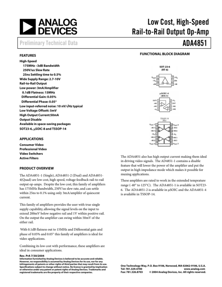
FUNCTIONAL BLOCK DIAGRAM
SOT-23-6
(RT-6)
APPLICATIONS
Consumer Video
Professional Video
Video Switchers
Active Filters
PRODUCT OVERVIEW
The ADA4851-1 (Single), ADA4851-2 (Dual) and ADA48514(Quad) are low cost, high speed, voltage feedback rail-to-rail
output op-amps. Despite the low cost, this family of amplifiers
has 175MHz Bandwidth, 250V/us slew rate, and can settle
within 25ns to 0.1% using only 3mA/amplifer of quiescent
current.
The ADA4851 also has high output current making them ideal
in driving video signals. The AD4851-1 contains a disable
feature that will lower the power of the amplifier and put the
output in high impedance mode which makes it possible for
muxing applications.
These amplifers are rated to work in the extended temprature
range (-40° to 125°C). The ADA4851-1 is available in SOT236. The ADA4851-2 is available in µSOIC and the ADA4851-4
is available in TSSOP-14.
This family of amplifiers provides the user with true single
supply capability, allowing the signal levels on the input to
extend 200mV below negative rail and 1V within positive rail.
On the output the amplifier can swing within 50mV of the
either rail.
With 0.1dB flatness out to 15MHz and Differential gain and
phase of 0.05% and 0.05° this family of amplifiers is ideal for
video applications.
Combining its low cost with performance, these amplifiers are
ideal in consumer applications.
Rev. PrA 7/30/2004
Information furnished by Analog Devices is believed to be accurate and reliable.
However, no responsibility is assumed by Analog Devices for its use, nor for any
infringements of patents or other rights of third parties that may result from its use.
Specifications subject to change without notice. No license is granted by implication
or otherwise under any patent or patent rights of Analog Devices. Trademarks and
registered trademarks are the property of their respective companies.
One Technology Way, P.O. Box 9106, Norwood, MA 02062-9106, U.S.A.
www.analog.com
Tel: 781.329.4700
Fax: 781.326.8703
© 2004 Analog Devices, Inc. All rights reserved.
ADA4851
Preliminary Technical Data
TABLE OF CONTENTS
ADA4851 Specifications .................................................................. 3
Thermal Resistance ...........................................................................6
ADA4851 Specifications .................................................................. 4
Outline Dimensions ..........................................................................7
ADA4851 Specifications .................................................................. 5
ESD Caution.......................................................................................7
Absolute Maximum Ratings............................................................ 6
REVISION HISTORY
Revision PrA: Initial Version
Rev. PrA | Page 2 of 8
Preliminary Technical Data
ADA4851
ADA4851 SPECIFICATIONS
Table 1. VS = +3 V (@TA = +25oC, G = +10, RL = 1 kΩ, unless otherwise noted.)
Parameter
DYNAMIC PERFORMANCE
–3 dB Bandwidth
Bandwidth for 0.1 dB Flatness
Slew Rate
Settling Time to 0.1%
NOISE/DISTORTION PERFORMANCE
Harmonic Distortion (dBc) HD2/HD3
Input Voltage Noise
Input Current Noise
Differential Gain
Differential Phase
DC PERFORMANCE
Input Offset Voltage
Input Offset Voltage Drift
Input Bias Current
Input Bias Current Drift
Input Bias Offset Current
Open-Loop Gain
INPUT CHARACTERISTICS
Input Resistance
Input Capacitance
Input Common-Mode Voltage Range
Common-Mode Rejection Ratio
DISABLE PIN
DISABLE Input Voltage
Turn-Off Time
Turn-On Time
OUTPUT CHARACTERISTICS
Output Overdrive Recovery Time (Rise/Fall)
Output Voltage Swing
Short-Circuit Current
POWER SUPPLY
Operating Range
Quiescent Current
Quiescent Current (Disabled)
Power Supply Rejection Ratio
Conditions
Min
Typ
Max
Unit
G = +1, VO = 0.2 V p-p
G = +1, VO = 2 V p-p
G = +1, VO = 2 V p-p
G = +1, VO = 2V Step
G = +2, VO = 2 V Step
175
25
15
250
25
MHz
MHz
MHz
V/µs
ns
fC = 1 MHz, VO = 2 V p-p,G = +1
f = 100 kHz
f = 100 kHz, DISABLE pin floating
G=+2
G=+2
75
9
1.5
0.05
0.05
dBc
nV/√Hz
pA/√Hz
%
°
5
10
1.8
10
0.1
Differential mode
300
1.4
-0.2 TO 2.0
100
VCM = +2 V
kΩ
pF
V
dB
Output disabled
V
ns
ns
VIN = ±1.5V, G =+2
RL = 150Ω
Sinking and Sourcing
Rev. PrA | Page 3 of 8
ns
V
mA
0.05 to 2.95
2.7
DISABLE = Low
Vs=1V
mV
µV/°C
µA
nA/°C
µA
dB
12
3
0.5
95
V
mA
mA
dB
ADA4851
Preliminary Technical Data
ADA4851 SPECIFICATIONS
Table 2. VS = +5 V (@TA = +25oC, G = +10, RL = 1 kΩ, unless otherwise noted.)
Parameter
DYNAMIC PERFORMANCE
–3 dB Bandwidth
Bandwidth for 0.1 dB Flatness
Slew Rate
Settling Time to 0.1%
NOISE/DISTORTION PERFORMANCE
Harmonic Distortion (dBc) HD2/HD3
Input Voltage Noise
Input Current Noise
Differential Gain
Differential Phase
DC PERFORMANCE
Input Offset Voltage
Input Offset Voltage Drift
Input Bias Current
Input Bias Current Drift
Input Bias Offset Current
Open-Loop Gain
INPUT CHARACTERISTICS
Input Resistance
Input Capacitance
Input Common-Mode Voltage Range
Common-Mode Rejection Ratio
DISABLE PIN
DISABLE Input Voltage
Turn-Off Time
Turn-On Time
OUTPUT CHARACTERISTICS
Output Overdrive Recovery Time (Rise/Fall)
Output Voltage Swing
Short-Circuit Current
POWER SUPPLY
Operating Range
Quiescent Current
Quiescent Current (Disabled)
Power Supply Rejection Ratio
Conditions
Min
Typ
Max
Unit
G = +1, VO = 0.2 V p-p
G = +1, VO = 2 V p-p
G = +1, VO = 2 V p-p
G = +1, VO = 2V Step
G = +2, VO = 2 V Step
175
25
15
250
25
MHz
MHz
MHz
V/µs
ns
fC = 1 MHz, VO = 2 V p-p,G = +1
f = 100 kHz
f = 100 kHz, DISABLE pin floating
G=+2
G=+2
75
9
1.5
0.05
0.05
dBc
nV/√Hz
pA/√Hz
%
°
5
10
1.8
10
0.1
Differential mode
300
1.4
-0.2 TO 4.0
100
VCM = +4 V
kΩ
pF
V
dB
Output disabled
V
ns
ns
VIN = ±1.5V, G =+2
RL = 150Ω
Sinking and Sourcing
Rev. PrA | Page 4 of 8
ns
V
mA
0.05 to 4.95
2.7
DISABLE = Low
Vs=3
mV
µV/°C
µA
nA/°C
µA
dB
12
3
0.5
95
V
mA
mA
dB
Preliminary Technical Data
ADA4851
ADA4851 SPECIFICATIONS
Table 3. VS = ±5 V (@TA = +25oC, G = +10, RL = 1 kΩ, unless otherwise noted.)
Parameter
DYNAMIC PERFORMANCE
–3 dB Bandwidth
Bandwidth for 0.1 dB Flatness
Slew Rate
Settling Time to 0.1%
NOISE/DISTORTION PERFORMANCE
Harmonic Distortion (dBc) HD2/HD3
Input Voltage Noise
Input Current Noise
Differential Gain
Differential Phase
DC PERFORMANCE
Input Offset Voltage
Input Offset Voltage Drift
Input Bias Current
Input Bias Current Drift
Input Bias Offset Current
Open-Loop Gain
INPUT CHARACTERISTICS
Input Resistance
Input Capacitance
Input Common-Mode Voltage Range
Common-Mode Rejection Ratio
DISABLE PIN
DISABLE Input Voltage
Turn-Off Time
Turn-On Time
OUTPUT CHARACTERISTICS
Output Overdrive Recovery Time (Rise/Fall)
Output Voltage Swing
Short-Circuit Current
POWER SUPPLY
Operating Range
Quiescent Current
Quiescent Current (Disabled)
Power Supply Rejection Ratio
Conditions
Min
Typ
Max
Unit
G = +1, VO = 0.2 V p-p
G = +1, VO = 2 V p-p
G = +1, VO = 2 V p-p
G = +1, VO = 2V Step
G = +2, VO = 2 V Step
175
25
15
250
25
MHz
MHz
MHz
V/µs
ns
fC = 1 MHz, VO = 2 V p-p,G = +1
f = 100 kHz
f = 100 kHz, DISABLE pin floating
G=+2
G=+2
75
9
1.5
0.05
0.05
dBc
nV/√Hz
pA/√Hz
%
°
5
10
1.8
10
0.1
Differential mode
300
1.4
-5.2 TO 5.0
100
VCM = +9 V
kΩ
pF
V
dB
Output disabled
V
ns
ns
VIN = ±1.5V, G =+2
RL = 150Ω
Sinking and Sourcing
Rev. PrA | Page 5 of 8
ns
V
mA
-4.95 to 4.95
2.7
DISABLE = Low
Vs=5
mV
µV/°C
µA
nA/°C
µA
dB
12
3
0.5
95
V
mA
mA
dB
ADA4851
Preliminary Technical Data
ABSOLUTE MAXIMUM RATINGS
Table 4. ADA4851 Absolute Maximum Ratings
Parameter
Supply Voltage
Power Dissipation
Common-Mode Input Voltage
Differential Input Voltage
Storage Temperature
Operating Temperature Range
Lead Temperature Range
(Soldering 10 sec)
Junction Temperature
Rating
12 V
See Figure 2
VEE – 0.5 V to VCC + 0.5 V
1.8 V
–65°C to +125°C
–40°C to +85°C
300°C
150°C
Stresses above those listed under Absolute Maximum Ratings
may cause permanent damage to the device. This is a stress
rating only and functional operation of the device at these or
any other condition s above those indicated in the operational
section of this specification is not implied. Exposure to absolute
maximum rating conditions for extended periods may affect
device reliability.
THERMAL RESISTANCE
stresses that the package exerts on the die, permanently shifting
the parametric performance of the ADA4851. Exceeding a
junction temperature of 175°C for an extended period of time
can result in changes in the silicon devices potentially causing
failure.
The power dissipated in the package (PD) is the sum of the
quiescent power dissipation and the power dissipated in the
package due to the load drive for all outputs. The quiescent
power is the voltage between the supply pins (VS) times the
quiescent current (IS). Assuming the load (RL) is mid-supply,
then the total drive power is VS/2 × IOUT, some of which is
dissipated in the package and some in the load (VOUT × IOUT).
RMS output voltages should be considered. If RL is referenced to
VS- as in single supply operation, the total power is VS × IOUT.
In single supply with RL to VS- worst case is VOUT = VS/2.
Airflow will increase heat dissipation effectively reducing θJA.
Also, more metal directly in contact with the package leads
from metal traces, through holes, ground, and power planes will
reduce the θJA.
θJA is specified for the worst-case conditions, i.e., θJA is specified
for device soldered in circuit board for surface mount packages.
Table 5. Thermal Resistance
Package Type
SOT23-6
µSOIC-8
TSSOP-14
θJA
180
150
°C/W
°C/W
120
°C/W
Unit
Maximum Power Dissipation
The maximum safe power dissipation in the ADA4851 package
is limited by the associated rise in junction temperature (TJ) on
the die. At approximately 150°C, which is the glass transition
temperature, the plastic will change its properties. Even
temporarily exceeding this temperature limit may change the
Rev. PrA | Page 6 of 8
Preliminary Technical Data
ADA4851
OUTLINE DIMENSIONS
Figure 1. SOT23-6—Dimensions shown in millimeters
Figure 2. µSOIC-8 —Dimensions shown in millimeters
Figure 3. TSSOP-14 ---- Dimensions shown in millimeters
ESD CAUTION
ESD (electrostatic discharge) sensitive device. Electrostatic charges as high as 4000 V readily accumulate on the
human body and test equipment and can discharge without detection. Although this product features
proprietary ESD protection circuitry, permanent damage may occur on devices subjected to high energy
electrostatic discharges. Therefore, proper ESD precautions are recommended to avoid performance
degradation or loss of functionality.
Rev. PrA | Page 7 of 8
ADA4851
Preliminary Technical Data
Table 6. Ordering Guide
ADA4851 Products
ADA4851-1ART-R2
Temperature Package
–40°C to +125°C
Package Description
6-Lead SOT-23
Package Outline
RT-6
Branding
HHB
ADA4851-1ART-REEL
–40°C to +125°C
6-Lead SOT-23
RT-6
HHB
ADA4851-1ART-REEL7
–40°C to +125°C
6-Lead SOT-23
RT-6
HHB
ADA4851-2ARM
–40°C to +125°C
8-Lead µSOIC
RM-8
HIB
ADA4851-2ARM-REEL
–40°C to +125°C
8-Lead µSOIC
RM-8
HIB
ADA4851-2ARM-REEL7
–40°C to +125°C
RM-8
HIB
ADA4851-4ARU
–40°C to +125°C
8-Lead µSOIC
14-Lead TSSOP
ADA4851-4ARU-REEL
–40°C to +125°C
14-Lead TSSOP
RU-14
ADA4851-4ARU-REEL7
–40°C to +125°C
14-Lead TSSOP
RU-14
Rev. PrA | Page 8 of 8
RU-14


